Circuit board and implementation method for interlayer interconnection structure thereof and processing method for circuit board

A technology of interlayer interconnection and implementation method, which is applied in the direction of printed circuit, printed circuit, printed circuit manufacturing, etc., can solve the problems of high cost, poor reliability, low efficiency, etc., achieve high reliability, improve reliability, and reduce production cost effect

Inactive Publication Date: 2015-07-01
SHENNAN CIRCUITS
View PDF6 Cites 2 Cited by
  • Summary
  • Abstract
  • Description
  • Claims
  • Application Information

AI Technical Summary

Problems solved by technology

[0008] Embodiments of the present invention provide a method for realizing the interlayer interconnection structure of a circuit board, a related circuit board and a processing method for the circuit board, so as to solve the problems of poor reliability, low efficiency and high cost existing in the existing blind hole filling and leveling technology

Method used


Image

  • Circuit board and implementation method for interlayer interconnection structure thereof and processing method for circuit board
  • Circuit board and implementation method for interlayer interconnection structure thereof and processing method for circuit board
  • Circuit board and implementation method for interlayer interconnection structure thereof and processing method for circuit board

Examples


Embodiment 1

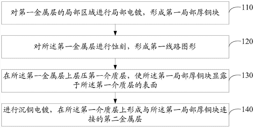
[0046] Please refer to Figure 1a , an embodiment of the present invention provides a method for realizing an interconnection structure between layers of a circuit board, which may include:

[0047] 110. Perform local electroplating on a local area of ​​the first metal layer to form a first interlayer interconnection block.

[0048] The circuit board as the processing object initially includes at least the first metal layer. In this step, local electroplating is performed on the local area of ​​the first metal layer that needs to be interconnected between layers, and the local area is electroplated thicker to form the The first inter-layer interconnect block required.

[0049] 120. Etch the first metal layer to form a first circuit pattern.

[0050] In this step, a conventional process, such as an inner layer pattern etching method, can be used to cover the area of ​​the first metal layer that needs to form a circuit pattern with a resist film, and then perform etching to rem...

Embodiment 2

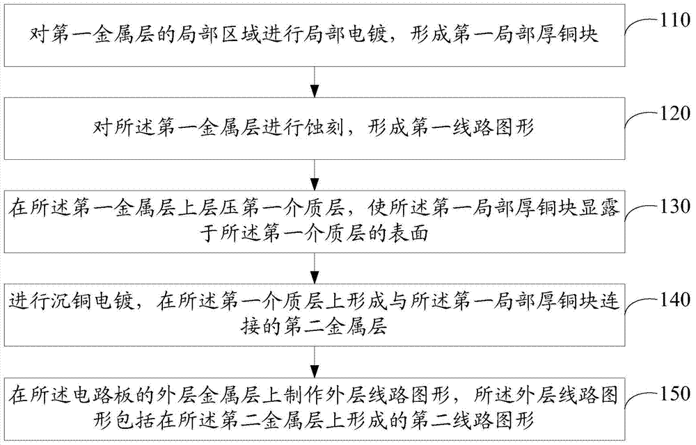
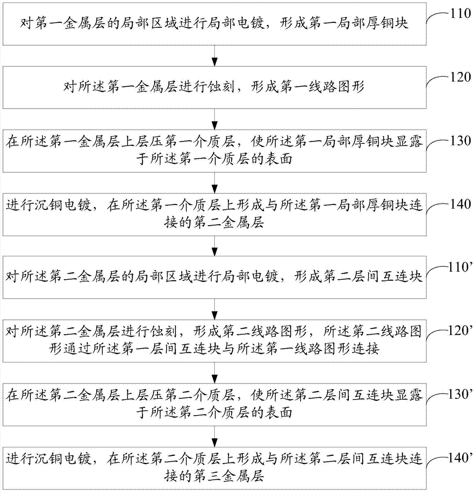
[0080] Please refer to figure 2 , an embodiment of the present invention provides a method for realizing an interconnection structure between layers of a circuit board, which may include:

[0081] 210. Perform local electroplating on a local area of ​​the first metal layer to form a first interlayer interconnection block.

[0082] The method of the embodiment of the present invention can start processing based on the inner layer board, and the said inner layer board includes at least one zeroth dielectric layer and at least one metal layer. In this embodiment, the inner layer board is double-sided copper-clad board as an example for illustration, as image 3 As shown, the inner board includes a first metal layer 21 on the first surface, a zeroth metal layer 20 on the second surface, and a zeroth metal layer between the zeroth metal layer 20 and the first metal layer 21. Dielectric layer 19. In other embodiments, at least one inner circuit layer and at least two zeroth diel...

Embodiment 3

[0120] Please refer to Figure 4d and 4e , an embodiment of the present invention provides a circuit board with an interlayer interconnection structure, the circuit board may include:

[0121] The first circuit layer 210, the first dielectric layer 18a disposed on the first circuit layer 210, and the second circuit layer 220 formed on the first dielectric layer 18a; wherein, the first circuit layer 210 includes a first interlayer interconnection block 31, and the first interlayer interconnection block 31 is connected to the second circuit layer 220 through the first dielectric layer 18a.

[0122] In some embodiments of the present invention, the circuit board may further include:

[0123] The second dielectric layer 18b disposed on the second circuit layer 220, and the third circuit layer 230 formed on the second dielectric layer 18b; wherein, the second circuit layer 220 includes a second interlayer interconnect The connection block 32, the second interlayer interconnectio...


PUM


Abstract

The invention discloses an implementation method for an interlayer interconnection structure of a circuit board and related circuit board and a processing method for the circuit board, and solves the problems of existing blind hole filling technology of poor reliability, low efficiency and high cost. The circuit board comprises a first metal layer; the method comprises the following steps: partially electroplating partial region of the first metal layer for forming a first interlayer interconnection block; etching the first metal layer for forming a first line figure; laminating a first dielectric layer on the first metal layer for exposing the first interlayer interconnection block on the surface of the first dielectric layer; copper deposition electroplating for forming a second metal layer on the first dielectric layer, and the second metal layer is connected with the first interlayer interconnection block.

Description

technical field [0001] The invention relates to the technical field of circuit boards, in particular to a method for realizing an interlayer interconnection structure of a circuit board, a related circuit board, and a processing method for the circuit board. Background technique [0002] HDI (High Density Interconnect, high-density interconnection or interconnection at any level) circuit boards are generally manufactured using blind hole filling technology. Connection, and then lamination build-up; by repeating the steps of drilling blind holes, electroplating filling and lamination, the connection of any two circuit layers can be realized. [0003] Practice has found that the above blind hole filling technology has the following defects: [0004] 1. Blind hole filling requires a special electroplating production line, and the electroplating production line that can be used for electroplating to fill blind holes has the characteristics of low production efficiency and high ...

Claims


Application Information

Patent Timeline
Patent Type & Authority Applications(China)
IPC IPC(8): H05K1/11H05K3/40
CPCH05K3/425H05K3/4652H05K2201/09563
Inventor 丁大舟缪烨刘宝林
Owner SHENNAN CIRCUITS
Why Eureka
Try Eureka