Wafer edge defect detection method

A technology of edge defects and detection methods, applied in semiconductor/solid-state device testing/measurement, electrical components, circuits, etc., can solve problems such as gaps, chip yield loss, etc., and achieve the effect of fast scanning and sensitivity

Active Publication Date: 2015-07-08
SHANGHAI HUALI MICROELECTRONICS CORP
View PDF6 Cites 8 Cited by
  • Summary
  • Abstract
  • Description
  • Claims
  • Application Information

AI Technical Summary

Problems solved by technology

Moreover, since the wafer edge is often in contact with the manipulators of different process equipment, chips may be generated due to collisions
Due to the direct contact between the wafer and the liquid water during the immersion lithography exposure process, the defects existing on the edge of the wafer may be transported to the front of the wafer through the liquid water, resulting in the formation of various pattern-related defects in the subsequent exposure process , resulting in a large loss of chip yield

Method used


Image

  • Wafer edge defect detection method
  • Wafer edge defect detection method
  • Wafer edge defect detection method

Examples


Embodiment Construction

[0033] The specific embodiment of the present invention will be further described in detail below in conjunction with the accompanying drawings.

[0034] It should be noted that, in the following specific embodiments, when describing the embodiments of the present invention in detail, in order to clearly show the structure of the present invention for the convenience of description, the structures in the drawings are not drawn according to the general scale, and are drawn Partial magnification, deformation and simplification are included, therefore, it should be avoided to be interpreted as a limitation of the present invention.

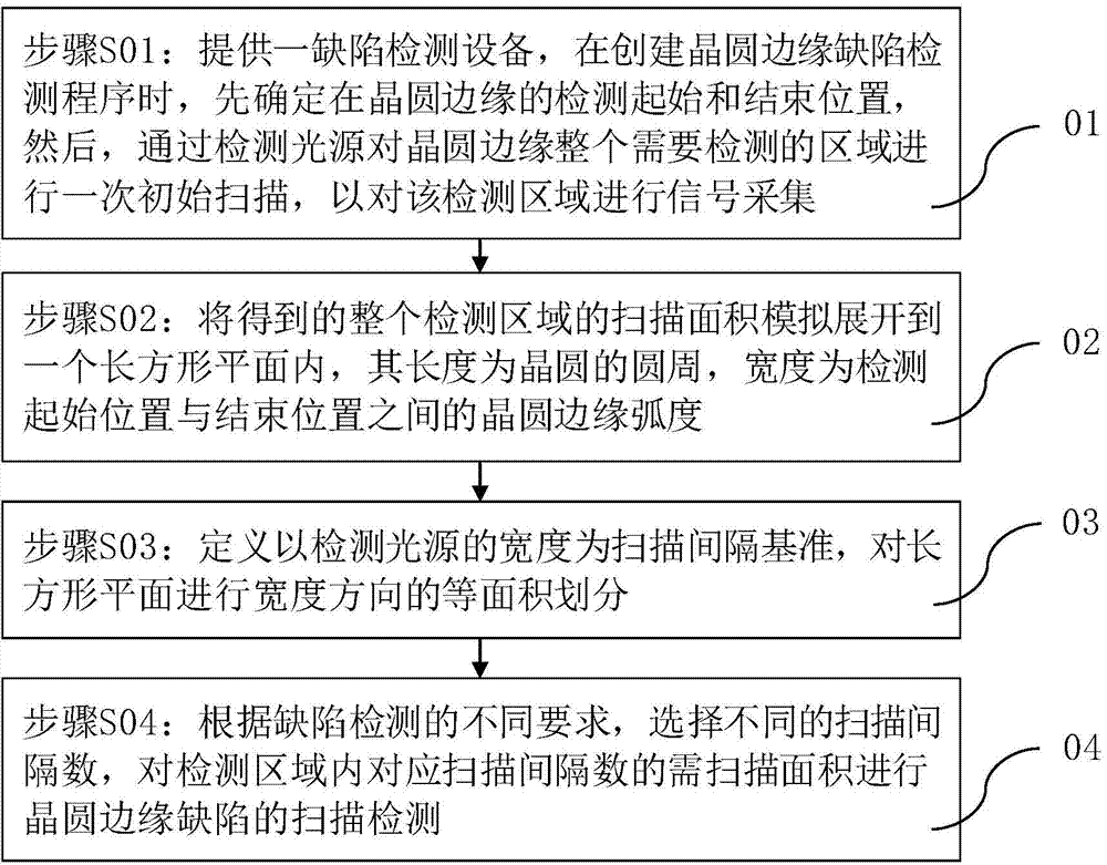
[0035] In the following specific embodiments of the present invention, please refer to image 3 , image 3 It is a flowchart of a method for detecting wafer edge defects in the present invention; at the same time, please refer to figure 2 and Figure 4 ~ Figure 9 , figure 2 and Figure 4 ~ Figure 9 yes to use image 3 Demonstrative descriptio...


PUM


Abstract

The invention discloses a wafer edge defect detection method. When a wafer edge defect detection program is created, signals of a whole detection region of the wafer edge are acquired firstly, the scanning area of the acquired whole detection region is simulated and expanded into a rectangular plane, the width of a detection light source serves as a scanning interval criterion so that the rectangular plane can be divided according to the equal area, according to different requirements of defect detection, different scanning interval numbers are selected for conducting scanning detection on wafer edge defects, according to the flexibility requirements of different defects, wafer edge scanning methods conducted at different speeds are flexibly selected, rapid scanning operation is achieved, and detection flexibility is considered as well.

Description

technical field [0001] The invention relates to the technical field of detection of semiconductor integrated circuits, and more particularly relates to a method capable of rapidly detecting wafer edge defects. Background technique [0002] When the critical dimension of the device enters below 45 nanometers, the traditional dry lithography technology cannot meet the production process requirements due to the limit of resolution, and the immersion lithography process will become larger due to its superior technical performance and good cost performance scale into production. [0003] see figure 1 , figure 1 is a schematic diagram of the cross-sectional structure of the wafer edge. like figure 1 As shown, the topography of the edge of the wafer 1 includes three regions, namely the upper bevel 2 , the top surface 3 and the lower bevel 4 . Since the edge area is not precisely controlled by the process in the production process of the integrated circuit, some extra thin film...

Claims


Application Information

Patent Timeline
Patent Type & Authority Applications(China)
IPC IPC(8): H01L21/66
CPCH01L22/20
Inventor 倪棋梁陈宏璘龙吟
Owner SHANGHAI HUALI MICROELECTRONICS CORP
Why Eureka
Try Eureka