

GaN nanowire and preparation method thereof
A technology of nanowires and thin films, applied in the field of GaN nanowires and its preparation, nanowire microelectronics and optoelectronic devices, can solve the problems of difficult control of the radius, height and growth position of GaN nanowires, and achieve low cost and operability strong effect
- Summary
- Abstract
- Description
- Claims
- Application Information
AI Technical Summary
Problems solved by technology
Method used
Image

Examples
Embodiment 1
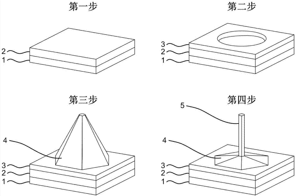
[0039] A GaN nanowire with a diameter of less than 200 nm and a height of about 5 μm is prepared on a Si substrate. The material structure of this embodiment is from bottom to top, Si substrate, AlN group III nitride film, SiO 2 Patterned masking film, GaN nanowires. That is, in this embodiment, the substrate 1 is an Si substrate, the group III nitride film 2 is an AlN group III nitride film, and the patterned masking film 3 is SiO 2 Graphical masking film.
[0040] The preparation method sequentially includes the following steps:
[0041] Step 1: Put the Si substrate into the MOCVD reaction chamber, and epitaxially grow an AlN group III nitride film with a thickness of 300 nm on the Si substrate;
[0042] Step 2: By PECVD, deposit SiO with a thickness of 100 nm on the AlN group III nitride film (the AlN film grown on the Si substrate is an epitaxial wafer) 2 Dielectric layer, and use conventional photolithography and wet etching methods to remove SiO 2 The dielectric layer is prepar...
Embodiment 2
[0046] A GaN nanowire with a diameter of about 500 nm and a height of about 4 μm is prepared on a Si substrate. The material structure of this embodiment is from bottom to top, Si substrate, AlN / GaN group III nitride film, SiO 2 Patterned masking film, GaN nanowires. That is, in this embodiment, the substrate 1 uses a Si substrate, the group III nitride film 2 uses an AlN / GaN group III nitride film, and the patterned masking film 3 uses SiO 2 Graphical masking film.
[0047] The preparation method sequentially includes the following steps:
[0048] Step 1: Put the Si substrate into the MOCVD reaction chamber, and then epitaxially grow an AlN epitaxial layer with a thickness of 100 nm and a GaN epitaxial layer with a thickness of 800 nm on the Si substrate;
[0049] Step 2: Deposit 100 nm SiO on the AlN / GaN group III nitride film (the AlN / GaN film grown on the Si substrate is an epitaxial wafer) by PECVD 2 Dielectric layer, and use conventional photolithography and wet etching methods...
Embodiment 3
[0053] A GaN nanowire array with a diameter of less than 200 nm and a height of about 5 μm was prepared on a Si substrate. This embodiment uses a material structure that is basically the same as that of Embodiment 1. The material structure from bottom to top is Si substrate, AlN group III nitride film, SiO 2 Patterned masking film, GaN nanowires. That is, in this embodiment, the substrate 1 is an Si substrate, the group III nitride film 2 is an AlN group III nitride film, and the patterned masking film 3 is SiO 2 Graphical masking film.
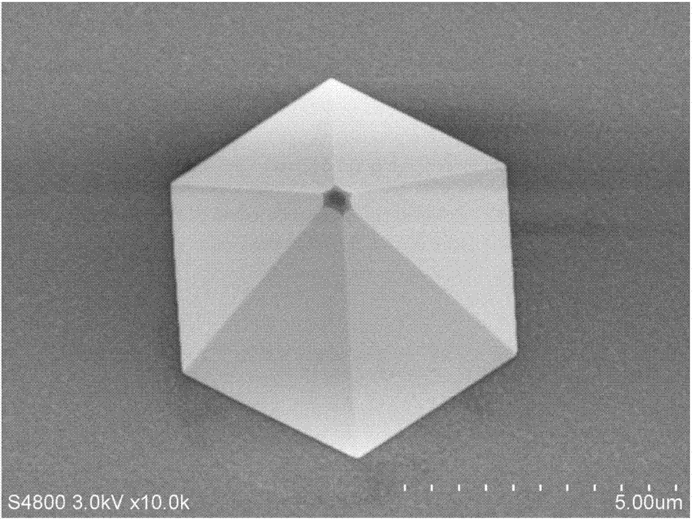
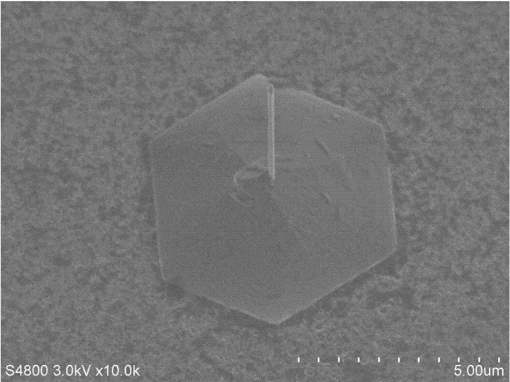
[0054] The specific preparation process is basically the same as that in Example 1. When the patterned masking film 3 is prepared in step 2, the pattern of the masking film is prepared into circular holes arranged periodically, the diameter of the circular holes is 3 μm, and the period is 10 μm. Therefore, the GaN hexagonal pyramid microstructure arranged in an array can be epitaxially grown in the subsequent MOCVD selective area growth process,...
PUM
| Property | Measurement | Unit |
|---|---|---|
| Hole diameter | aaaaa | aaaaa |
| Hole diameter | aaaaa | aaaaa |
Abstract
Description
Claims
Application Information