IGBT having super junction structure and preparation method thereof

A gate trench and collector technology, applied in the field of IGBT, can solve problems such as large saturation voltage drop, and achieve the effects of reducing saturation voltage drop, increasing breakdown voltage, and shortening processing time

Active Publication Date: 2015-07-15
SHANGHAI TUNA ELECTRIC MECHANIC EQUIP CO LTD
4 Cites 0 Cited by

AI-Extracted Technical Summary

Problems solved by technology

However, there is still a serious defect in this structure, that is, the electric field is distributed in one dimension in silicon, that i...

Method used

The advantage that the present invention implements: the IGBT with superjunction structure described in the present invention retains original structure, and adopts to set up P-type region and insulating medium filling region under gate trench, and this P-type region is respectively connected with The gate trench is connected to the P-type collector, so as to form a lateral electric field distribution between the P-type regions under two adjacent gate trenches, that is, the X-axis direction. According to the superjunction theory, almost every ionized donor’s positive The electric flux generated by the charge is absorbed by the negative charge of the nearby ionized acceptor, that is, the electric force line is horizontal, that is to...

Abstract

The present invention discloses an IGBT having with a super junction structure. The IGBT having the super junction structure comprises a collector, a drift region, a P-type base region and an N-type emitter region, wherein, gate grooves are formed in the P-type base region and the N-type emitter region, gate electrodes being arranged in the gate grooves; P-type regions are formed between the bottom of the gate grooves and the collector; the P-type regions are respectively connected with the bottom of the gate grooves and the collector; and spaces between the adjacent P-type regions are filled with an insulating medium. The present invention further discloses a preparation method of the IGBT having the super junction structure. The IGBT having the super junction structure provided by the present invention can generate a transverse electric field so as to improve the breakdown voltage and reduce the saturation voltage drop of a device. The preparation method provided by the present invention has the advantage of short processing time.

Application Domain

Technology Topic

Saturation voltageElectric field +3

Image

  • IGBT having super junction structure and preparation method thereof
  • IGBT having super junction structure and preparation method thereof
  • IGBT having super junction structure and preparation method thereof

Examples

  • Experimental program(1)

Example Embodiment

[0029] The technical solutions in the embodiments of the present invention will be clearly and completely described below in conjunction with the accompanying drawings in the embodiments of the present invention. Obviously, the described embodiments are only a part of the embodiments of the present invention, rather than all the embodiments. Based on the embodiments of the present invention, all other embodiments obtained by those of ordinary skill in the art without creative work shall fall within the protection scope of the present invention.
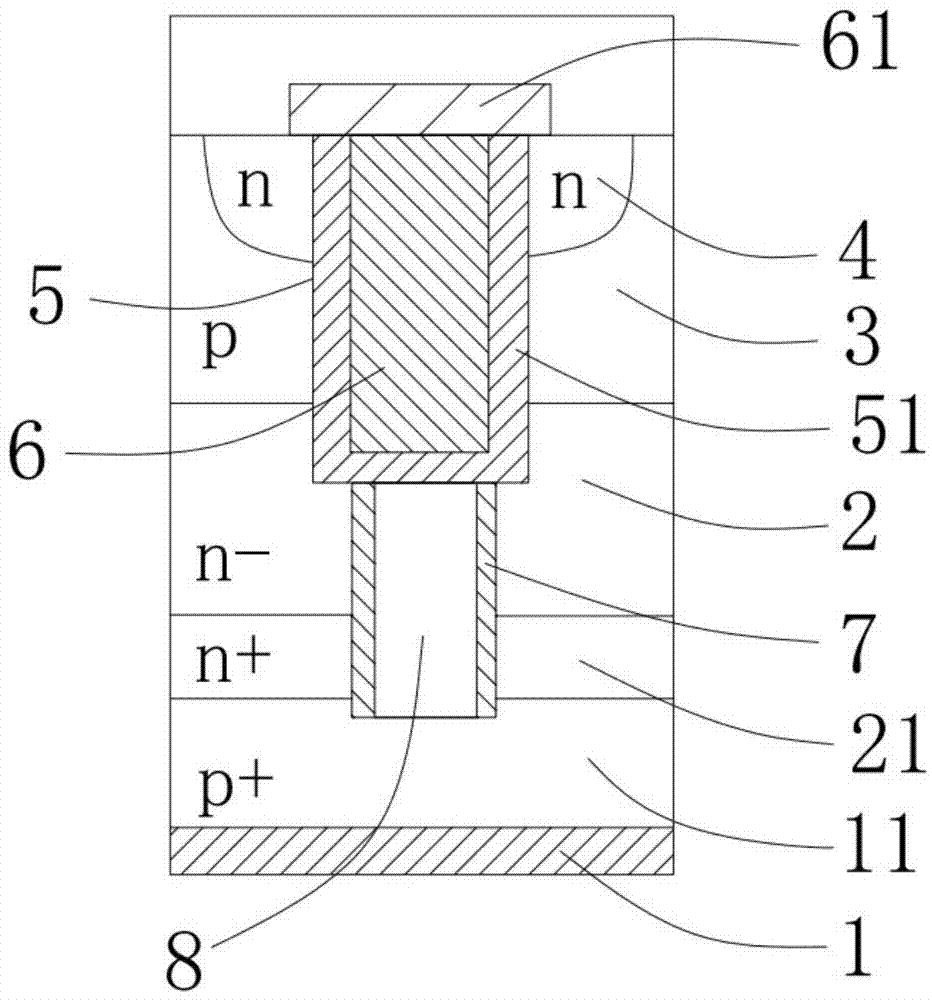
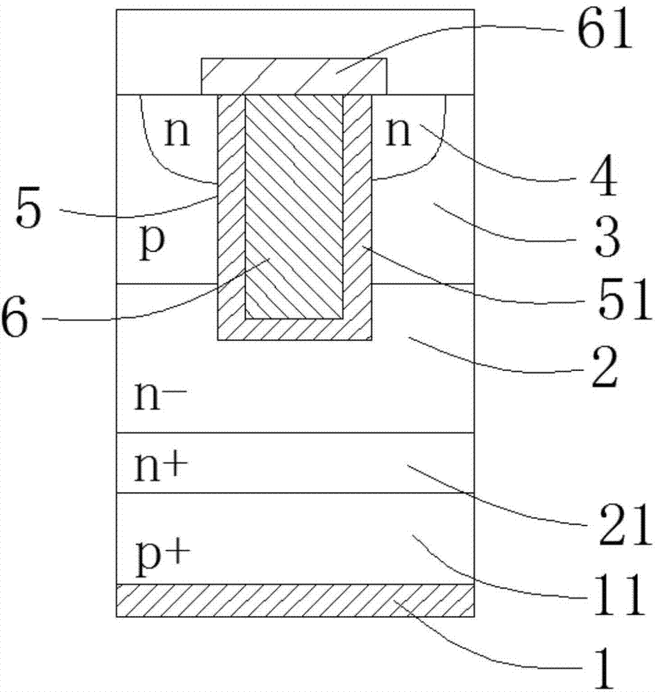
[0030] Such as figure 1 As shown, an IGBT with a super junction structure includes a collector 1, a drift region 2, a P-type base region 3, and an N-type emitter region 4. The P-type base A gate trench 5 is provided in the region 3 and the N-type emitter region 4, a gate electrode 6 is provided in the gate trench 5, and a P-type is provided between the bottom of the gate trench 5 and the collector 1 Area 7, the P-type area 7 is respectively connected to the bottom of the gate trench 5 and the collector 1, and the adjacent P-type area 7 is filled with an insulating medium 8; this solution retains the original structure , And add a P-type area 7 and an insulating medium 8 filling area under the gate trench 5. The P-type area 7 is connected to the gate trench 5 and the P-type collector 1 respectively, so that the two adjacent gate trenches 5 A horizontal electric field distribution is formed between the P-type regions 7 below, that is, in the X-axis direction. According to the superjunction theory, the electric flux generated by the positive charge of almost every ionized donor is affected by the negative charge of the nearby ionized acceptor. The absorbed, that is, the lines of electric force are lateral, that is to say, the electric field of the drift region 2 is two-dimensionally distributed. This mutual compensation relationship between the lateral charges can be roughly regarded as intrinsic to the longitudinal direction, which makes the doping concentration of each region very high, so the conductivity of the drift region 2 is very large when it is turned on, which effectively The saturation voltage drop of the IGBT is reduced and the breakdown voltage is increased.
[0031] Wherein, a gate oxide layer 51 is provided between the gate electrode 6 and the gate trench 5; an insulating layer 61 is provided on the top of the gate electrode; the insulating medium 8 may be silicon dioxide or polysilicon; the collector 1 A P+ collector region layer 11 and a buffer layer 21 are also provided between the drift region 2 and the collector electrode 1 and the P+ collector region layer 11, and the buffer layer 21 is adjacent to the drift region 2;
[0032] A preparation method of an IGBT with a super junction structure, the preparation method comprising the following steps:
[0033] Step 1: Epitaxy the N buffer layer and the N-drift zone layer on the P+ collector zone layer substrate;
[0034] Such as image 3 As shown, an N+ type buffer layer 200 and an N- type drift layer 300 are epitaxially grown on the main surface of the p+ type collector region layer substrate 100 in sequence.
[0035] Step 2: Making P-type base layer and N+ emitter layer;
[0036] Such as Figure 4 As shown, continue to extend the P-type base layer 400 and the N+ emitter layer 500 on the N-type drift layer 300.
[0037] Step 3: Form trenches by etching from the N+ emitter layer to the P+ collector region layer;
[0038] Such as Figure 5 As shown, the trench 600 is formed by forming a mask such as a resist on the upper surface of the N+ type emitter layer 500 in a region where the trench is not formed, and then performing partial etching in the thickness direction thereof. For example, the etching can be achieved by reactive ion etching (RIE), and inductively coupled plasma (ICP) RIE is particularly preferably used. For example, SF6 or a mixed gas of SF6 and O2 can be used as the reaction gas, and the etching can be realized by ICP-RIE.
[0039] Step 4: implant P on the sidewall of the trench to form a P-type region;
[0040] Such as Image 6 As shown, P is implanted into the sidewall of the trench 600 to form a P-type region 601, and large-angle ion implantation is used.
[0041] Step 5: Fill the trench with insulating medium;
[0042] Such as Figure 7 As shown, an insulating dielectric 602 is used to fill the trench 600, for example, silicon dioxide is used to fill the trench 600; for example, polysilicon is used to fill the trench 600.
[0043] Step 6: Continue to etch the larger gate trench on the filled trench;
[0044] Such as Figure 8 As shown, the larger gate trench 700 is continuously etched on the trench 600 that has been filled with an insulating medium such as silicon dioxide or polysilicon. For example, the etching can be achieved by reactive ion etching (RIE), and inductively coupled plasma (ICP) RIE is particularly preferably used. For example, SF6 or a mixed gas of SF6 and O2 can be used as the reaction gas, and the etching can be realized by ICP-RIE
[0045] Step 7: Add a gate oxide layer and a gate electrode in the gate trench;
[0046] Such as Picture 9 As shown, a gate oxide layer 701, which is an insulating film, is formed in the etched gate trench 700, and then deposited to form a gate electrode 702.
[0047] The step of implanting P into the sidewall of the trench to form the P-type region adopts a large-angle ion implantation method; the insulating medium used to fill the trench with an insulating medium is silicon dioxide; the adding in the gate trench The gate oxide layer and gate electrode are specifically: gate oxide and in-situ doped polycrystalline deposition
[0048] The advantages of the implementation of the present invention: the IGBT with a super junction structure of the present invention retains the original structure, and adopts an additional P-type region and an insulating dielectric filling region under the gate trench, and the P-type region is respectively the same as the gate trench It is connected to the P-type collector to form a lateral electric field distribution between the P-type regions under two adjacent gate trenches, that is, the X-axis direction. According to the superjunction theory, almost every ionized donor’s positive charge generates The electric flux is absorbed by the negative charge of the ionizing acceptor nearby, that is, the electric force line is lateral, that is to say, the electric field in the drift zone is two-dimensionally distributed. This mutual compensation relationship between the lateral charges can be roughly regarded as intrinsic to the vertical direction, which makes the doping concentration of each region very high, so the conductivity of the drift region during turn-on is very large, which effectively reduces The saturation voltage drop of the IGBT is increased, and the breakdown voltage is increased. The method for preparing an IGBT with a super junction structure provided by the present invention is that each zone layer is formed by stepwise epitaxy and ion implantation, and ion implantation is adopted, which is compared with the prior art , Has the advantage of short processing time.
[0049] The above are only specific embodiments of the present invention, but the scope of protection of the present invention is not limited to this. Any person skilled in the art can easily think of changes or substitutions within the technical scope disclosed in the present invention. All should be covered within the protection scope of the present invention. Therefore, the protection scope of the present invention should be subject to the protection scope of the claims.

PUM

no PUM

Description & Claims & Application Information

We can also present the details of the Description, Claims and Application information to help users get a comprehensive understanding of the technical details of the patent, such as background art, summary of invention, brief description of drawings, description of embodiments, and other original content. On the other hand, users can also determine the specific scope of protection of the technology through the list of claims; as well as understand the changes in the life cycle of the technology with the presentation of the patent timeline. Login to view more.

Similar technology patents

Miniature metal fully-sealed servo circuit of quartz flexible accelerometer and processing method of servo circuit

InactiveCN110579626AReduce weightReduce saturation pressure dropAcceleration measurementTransconductanceDifferential capacitance
Owner:XIAN MICROELECTRONICS TECH INST

Low-voltage and high-current reversing device based on H bridge

InactiveCN103414343AReduce saturation pressure dropFast current commutationApparatus without intermediate ac conversionSaturation voltageConstant current source
Owner:HARBIN INST OF TECH

Classification and recommendation of technical efficacy words

  • Improve breakdown voltage
  • Reduce saturation pressure drop

Carrier-storing grooved gate IGBT with P-type floating layer

InactiveCN101694850AReduce forward voltage dropImprove breakdown voltageSemiconductor devicesJFETHigh concentration
Owner:UNIV OF ELECTRONIC SCI & TECH OF CHINA

Miniature metal fully-sealed servo circuit of quartz flexible accelerometer and processing method of servo circuit

InactiveCN110579626AReduce weightReduce saturation pressure dropAcceleration measurementTransconductanceDifferential capacitance
Owner:XIAN MICROELECTRONICS TECH INST

Low-voltage and high-current reversing device based on H bridge

InactiveCN103414343AReduce saturation pressure dropFast current commutationApparatus without intermediate ac conversionSaturation voltageConstant current source
Owner:HARBIN INST OF TECH
Why Eureka
Try Eureka