IGBT and manufacturing method thereof

A manufacturing method and carrier storage technology, which is applied in the field of IGBT manufacturing, can solve the problems of long minority carrier life of IGBT, and achieve the effects of shortening minority carrier life, lowering saturation voltage, and reducing saturation voltage drop

Pending Publication Date: 2019-11-05
ADVANCED SEMICON MFG CO LTD
View PDF9 Cites 0 Cited by
  • Summary
  • Abstract
  • Description
  • Claims
  • Application Information

AI Technical Summary

Problems solved by technology

However, the minority-carrier lifetime of the IGBT manufactured by this method is longer

Method used


Image

  • IGBT and manufacturing method thereof
  • IGBT and manufacturing method thereof
  • IGBT and manufacturing method thereof

Examples


Embodiment Construction

[0039] The present invention will be further described below by means of a preferred embodiment, but the present invention is not limited to the scope of the described embodiment.

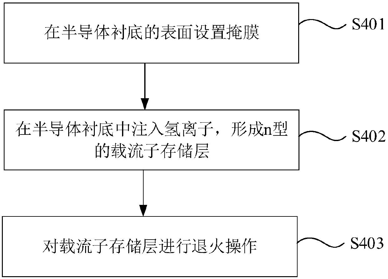
[0040] For the IGBT manufacturing method of this embodiment, refer to figure 2 , including the following steps:

[0041] S402, implanting hydrogen ions into the semiconductor substrate to form an n-type carrier storage layer.

[0042] In order to effectively implant hydrogen ions into the target area and avoid implanting hydrogen ions into non-target areas, such as figure 2 As shown, before hydrogen ion implantation, the IGBT manufacturing method of this embodiment includes the following steps:

[0043] S401, setting a mask on the surface of the semiconductor substrate, the mask includes a blocking area and a transmission area, the blocking area is used to block hydrogen ions from being implanted into the semiconductor substrate; the transmission area is used to allow hydrogen ions to pass thro...


PUM


Abstract

The invention discloses an IGBT and a manufacturing method thereof. The manufacturing method of the IGBT comprises the following steps of implanting hydrogen ions into a semiconductor substrate and forming an n-type carrier storage layer. According to the IGBT and the manufacturing method thereof disclosed by the invention, a hydrogen ion implantation technology is adopted in the step of fabricating the carrier storage layer, thereby playing a role of an n-type hole blocking layer after the carrier storage layer is formed and forming a recombination center. Therefore, a saturation voltage dropcan be reduced, and meanwhile, the minority carrier lifetime is effectively shortened.

Description

technical field [0001] The invention belongs to the technical field of IGBT (Insulated Gate Bipolar Transistor, insulated gate bipolar transistor) manufacturing, and in particular relates to an IGBT and a manufacturing method thereof. Background technique [0002] IGBT is a composite fully-controlled voltage-driven power semiconductor device composed of BJT (bipolar transistor) and MOS (insulated gate field effect transistor), and has MOSFET (Metal-Oxide-Semiconductor Field-EffectTransistor, metal-oxide The advantages of high input impedance of semiconductor field effect transistor) and low turn-on voltage drop of GTR (Giant Transistor, power transistor). The saturation voltage of GTR is low, the carrying current density is large, but the driving current is large; the driving power of MOSFET is small, the switching speed is fast, but the conduction voltage drop is large, and the current carrying density is small. The IGBT combines the advantages of the above two devices, wi...

Claims


Application Information

Patent Timeline
Patent Type & Authority Applications(China)
IPC IPC(8): H01L21/266H01L21/324H01L21/331
CPCH01L21/266H01L21/26506H01L21/324H01L29/66325
Inventor 王学良刘建华郎金荣
Owner ADVANCED SEMICON MFG CO LTD
Why Eureka
Try Eureka