Silicon germanium heterojunction bipolar transistor

A heterojunction bipolar, transistor technology, applied in semiconductor devices, semiconductor/solid-state device manufacturing, electrical components, etc., can solve the problem of increasing the size of the lateral lightly doped collector region, increasing the series resistance and saturation voltage drop, Increase the series resistance of the collector area to achieve the effect of reducing the series resistance, increasing the breakdown voltage, and reducing the lateral series resistance

Active Publication Date: 2013-07-24
SHANGHAI HUAHONG GRACE SEMICON MFG CORP
View PDF3 Cites 0 Cited by
  • Summary
  • Abstract
  • Description
  • Claims
  • Application Information

AI Technical Summary

Problems solved by technology

In RF high-voltage silicon-germanium heterojunction bipolar transistors (SiGe HBT), in order to maintain a high characteristic frequency under high breakdown voltage, the breakdown voltage of the transistor cannot be increased blindly by increasing the thickness of the lightly doped collector region. However, the pseudo-buried layers on both sides of the transistor are separated, and the breakdown voltage of the transistor is increased by relying on the two-dimensional distribution of the collector region / base junction depletion region, but the problem is that the size of the lateral lightly doped collector region increases. It also increases the series resistance of the collector region, so it also increases the saturation voltage drop, especially the shallow depth of the lightly doped collector region in the silicon under the field oxygen region, which further increases the series resistance and saturation voltage. drop

Method used


Image

  • Silicon germanium heterojunction bipolar transistor
  • Silicon germanium heterojunction bipolar transistor
  • Silicon germanium heterojunction bipolar transistor

Examples


Embodiment Construction

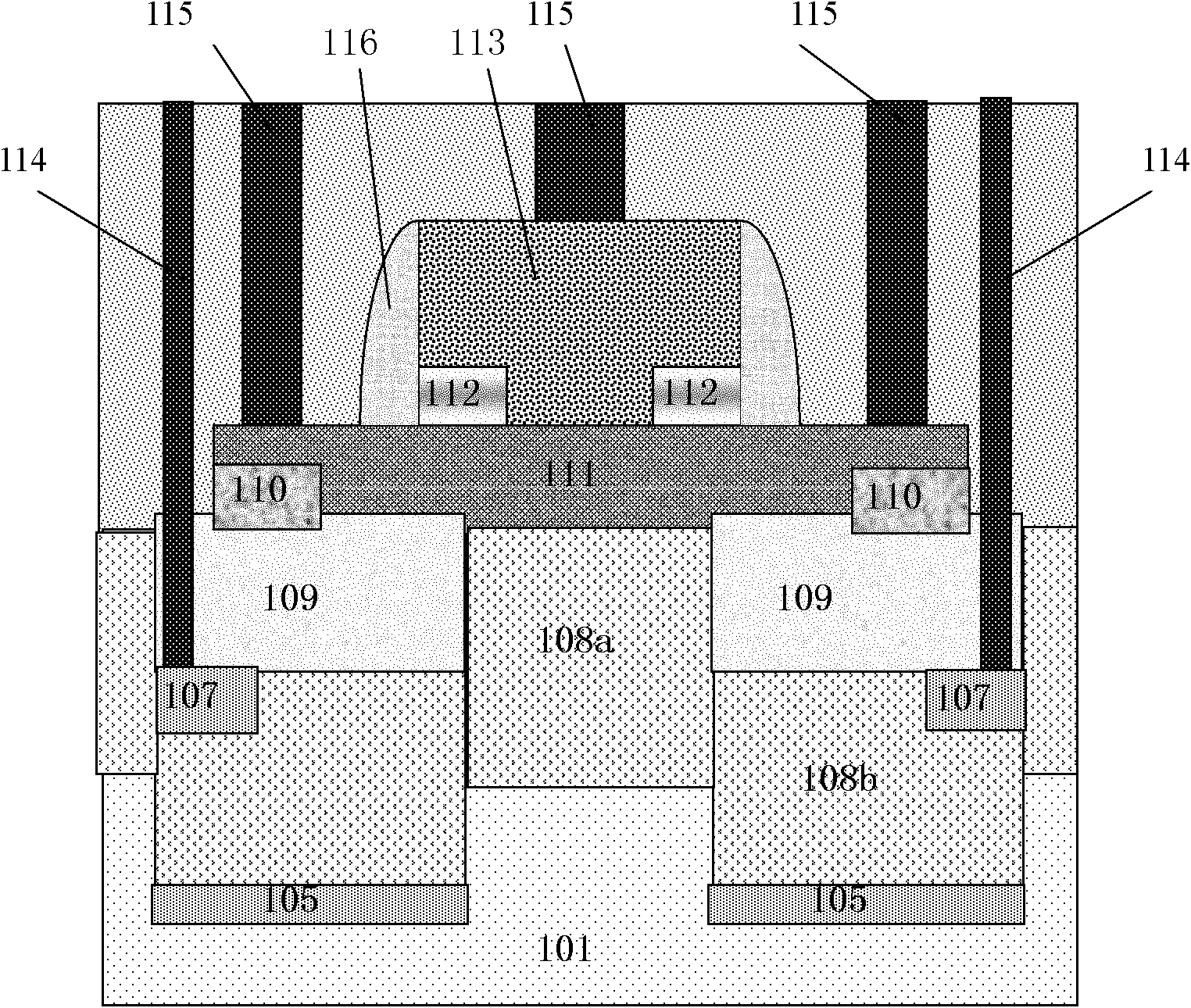
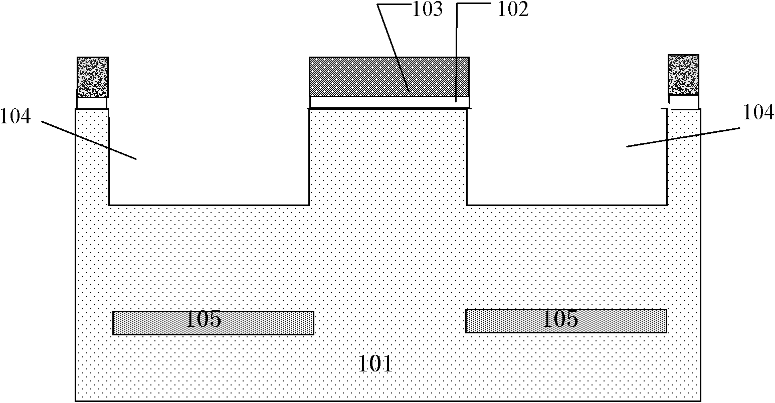
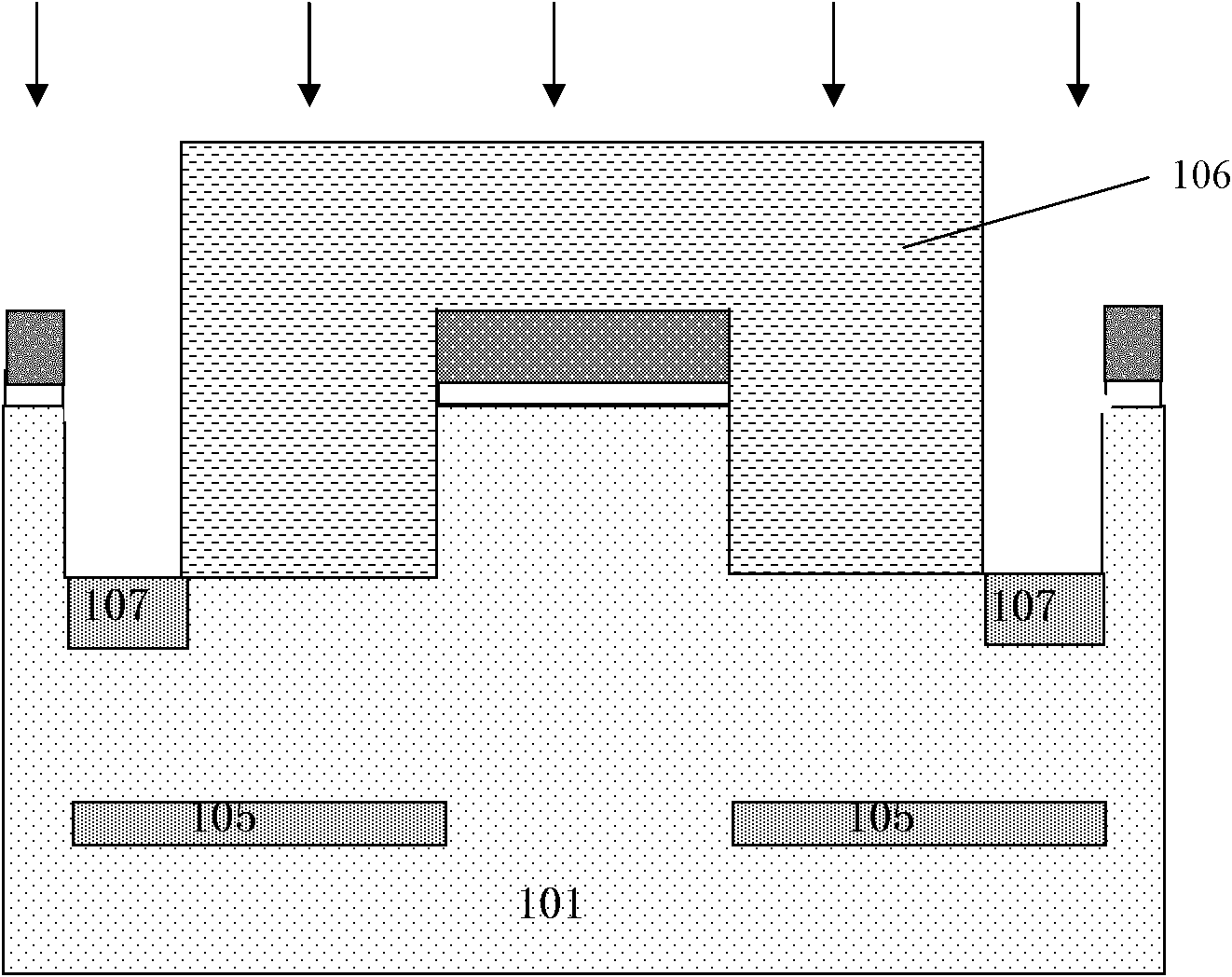
[0024] Such as figure 1 Shown is a schematic structural diagram of an embodiment of the present invention. The silicon-germanium heterojunction bipolar transistor in the embodiment of the present invention is formed on a P-type silicon substrate 101, and the active region is isolated by a field oxygen region 109. The silicon-germanium heterojunction bipolar transistor includes:

[0025] A collector region, consisting of ion implantation region 1 108a formed in the active region plus ion implantation region 2 108b and ion implantation region 3 formed at the bottom of the field oxygen region 109 on both sides of the active region 105; the first ion implantation area 108a, the second ion implantation area 108b, and the third ion implantation area 105 all have the first conductivity type; the third ion implantation area 105 is separated from the bottom surface of the field oxygen area 109 by a vertical The width of the deep pseudo-buried layer 107, the ion implantation region 3 1...


PUM


Abstract

The invention discloses a silicon germanium heterojunction bipolar transistor. The collector region of the silicon germanium heterojunction bipolar transistor consists of a first ion-implanted region which is formed in an active region, and second and third ion-implanted regions which are formed at the bottoms of field oxide regions on the two sides of the active region respectively. The third ion-implanted region is at a longitudinal distance away from the bottom surface of the field oxide region, and the width of the third ion-implanted region is the same as that of the field oxide region. The second ion-implanted region is positioned at the top of the ion-implanted region, and the bottom of the second ion-implanted region is overlapped and connected with the third ion-implanted region.The depth of the first ion-implanted region is greater than the depth of the bottom of the field oxide region, and the bottom of the first ion-implanted region is connected with the second ion-implanted region. The dosage concentration of the third ion-implanted region is greater than that of each of the first and second ion-implanted regions. Deep hole contact in the field oxide region at the top of a pseudo buried layer leads the collector region out. By the silicon germanium heterojunction bipolar transistor, the breakdown voltage of a device can be increased, relatively higher characteristic frequency can be maintained, the series resistance of the collector region can be decreased and the saturation voltage drop of the device can be decreased.

Description

technical field [0001] The invention relates to a semiconductor integrated circuit device, in particular to a germanium-silicon heterojunction bipolar transistor. Background technique [0002] Saturation voltage drop (Vcesat) is an important performance parameter of bipolar transistors, which reflects the size of Vce required for the transistor to enter the linear region under a certain collector current, so it is directly related to the DC power consumption of the transistor during normal operation. Reducing the saturation voltage drop is a necessary means to reduce the DC power consumption of bipolar transistors, especially for high-voltage bipolar transistors. In RF high-voltage silicon-germanium heterojunction bipolar transistors (SiGe HBT), in order to maintain a high characteristic frequency under high breakdown voltage, the breakdown voltage of the transistor cannot be increased blindly by increasing the thickness of the lightly doped collector region. However, the p...

Claims


Application Information

Patent Timeline
Patent Type & Authority Patents(China)
IPC IPC(8): H01L29/737H01L29/08H01L21/331
Inventor 钱文生
Owner SHANGHAI HUAHONG GRACE SEMICON MFG CORP
Why Eureka
Try Eureka