IGBT device with carrier storage structure and manufacturing method thereof

A carrier storage and device technology, applied in the field of IGBT devices, can solve the problems of reducing channel density, reducing product withstand voltage, bending of depletion layer, etc., reducing chip area, reducing chip cost, and reducing the peak value of surface electric field. Effect

Active Publication Date: 2019-02-15
WUXI NCE POWER
View PDF6 Cites 0 Cited by
  • Summary
  • Abstract
  • Description
  • Claims
  • Application Information

AI Technical Summary

Problems solved by technology

First of all, due to the existence of the inactive region of the second conductivity type region in the floating state, the channel density is reduced, so that the reduction of the conduction voltage drop (Vcesat) is limited; secondly, because the inactive region of the second conductivity type region is in the floating state, in When the device withstands the withstand voltage, the potential of the active region of the second conductivity type is inconsistent with that of the inactive region, so the depletion rate of the inactive region of the second conductivity type will be significantly slower than that of the active region of the second conductivity type. When the width of the active region of the second conductivity type is close to or greater than the width of the second conductivity type inactive region, the depletion layer will be significantly bent, and the product withstand voltage will be significantly reduced

Method used


Image

  • IGBT device with carrier storage structure and manufacturing method thereof
  • IGBT device with carrier storage structure and manufacturing method thereof
  • IGBT device with carrier storage structure and manufacturing method thereof

Examples


Embodiment Construction

[0049] The present invention will be further described below in conjunction with specific drawings and embodiments.

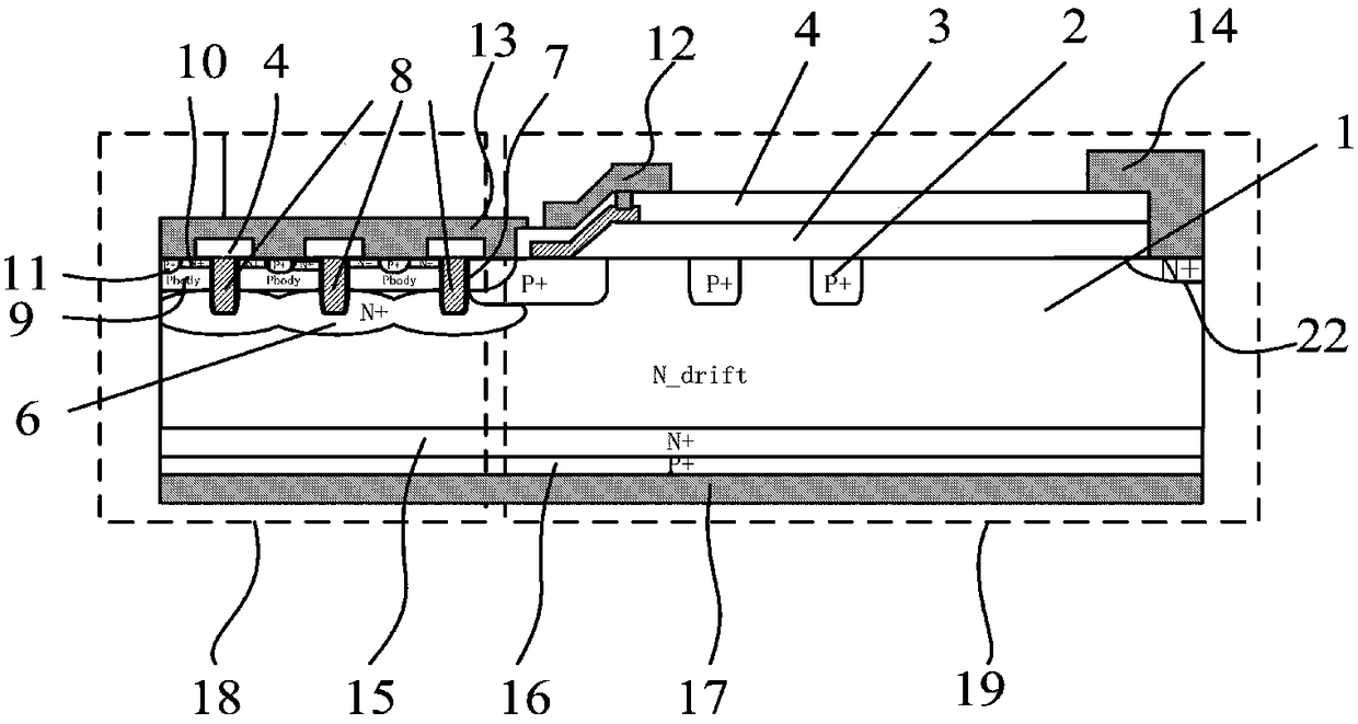
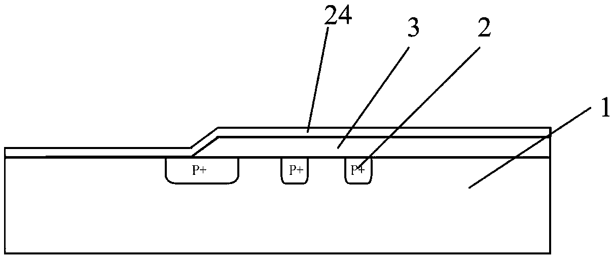
[0050] Such as figure 1 with Figure 9 Shown: In order to meet the low turn-on voltage drop (Vceon) and extremely fast turn-off characteristics at the same time, and to adjust the withstand voltage breakdown position to the cell area to ensure a higher voltage surge resistance ability, without increasing the cost of chip manufacturing. Taking N-type IGBT devices as an example, the present invention specifically includes: on the top view plane of the IGBT device, including the active region 18 and the terminal protection region 19 on the semiconductor substrate, the The active area 18 is located in the central area of ​​the semiconductor substrate, and the terminal protection area 19 is located at the outer circle of the active area 18 and surrounds the active area 18; on the cross section of the IGBT device, the semiconductor substrate has two opposite main T...


PUM


Abstract

The invention relates to an IGBT device with a carrier storage structure and a manufacturing method thereof. An active area of the IGBT device adopts a groove structure; a second conduction type body area is arranged in a first conduction type drifting area of the active area; a cellular groove is located in the second conduction type body area and deeply extends into the first conduction type drifting area below the second conduction type body area; the carrier storage structure is arranged in the first conduction type drifting area of the active area; the carrier storage structure comprises a first conduction type carrier storage area which is used for completely surrounding the inner and outer walls, extending in the first conduction type drifting area, of the cellular groove; and the doping concentration of the first conduction type carrier storage area is greater than the doping concentration of the first conduction type drifting area. According to the IGBT device with the carrier storage structure and the manufacturing method thereof, the relatively low breakover voltage drop and extremely rapid turnoff characteristic can be satisfied at the same time, the pressurization breakdown position can be adjusted to a cellular area to ensure relatively high voltage surge resistance, the chip manufacturing cost is not increased, and the chip area is reduced.

Description

technical field [0001] The invention relates to an IGBT device and a manufacturing method thereof, in particular to an IGBT device with a carrier storage structure and a manufacturing method thereof, belonging to the technical field of the IGBT device. Background technique [0002] The full name of IGBT is Insulate Gate Bipolar Transistor, which is an insulated gate bipolar transistor. It has many advantages of MOSFET and GTR, which greatly expands the application field of power semiconductor devices. As the main representative of new power semiconductor devices, IGBTs are widely used in the fields of industry, information, new energy, medicine, transportation, military and aviation. IGBT is one of the most important power devices at present. Due to the advantages of high input impedance, on-state voltage drop, simple drive circuit, wide safe working area, and strong current handling capability, IGBT has attracted more and more people in various power switch applications. a...

Claims


Application Information

Patent Timeline
Patent Type & Authority Patents(China)
IPC IPC(8): H01L29/739H01L29/06H01L29/10H01L29/423H01L21/331
CPCH01L29/06H01L29/10H01L29/423H01L29/66325H01L29/66477H01L29/739
Inventor 朱袁正张硕
Owner WUXI NCE POWER
Why Eureka
Try Eureka