Method for manufacturing power transistor

A technology of power transistors and manufacturing methods, applied in semiconductor/solid-state device manufacturing, electrical components, circuits, etc., can solve problems such as latch-up effect, unfavorable mass production, and opening of parasitic bipolar transistors, so as to improve the ability to resist latch-up , large current drive capability, and the effect of reducing the accumulation of holes

Active Publication Date: 2013-03-06
SHANGHAI HUAHONG GRACE SEMICON MFG CORP
View PDF4 Cites 0 Cited by
  • Summary
  • Abstract
  • Description
  • Claims
  • Application Information

AI Technical Summary

Problems solved by technology

However, the alignment deviation between different masks prevents the size of the device from being reduced according to demand, and the more precise photolithography technology makes the manufacturing cost expensive, which is not conducive to mass production.
In addition, when the hole current in the well region reaches a certain level, the potential of the well region will be raised, and the source-well junction barrier will be lowered, causing the parasitic bipolar transistor to be turned on. At this time, the gate cannot control the current switch, and a latch occurs effect

Method used


Image

  • Method for manufacturing power transistor
  • Method for manufacturing power transistor
  • Method for manufacturing power transistor

Examples


Embodiment Construction

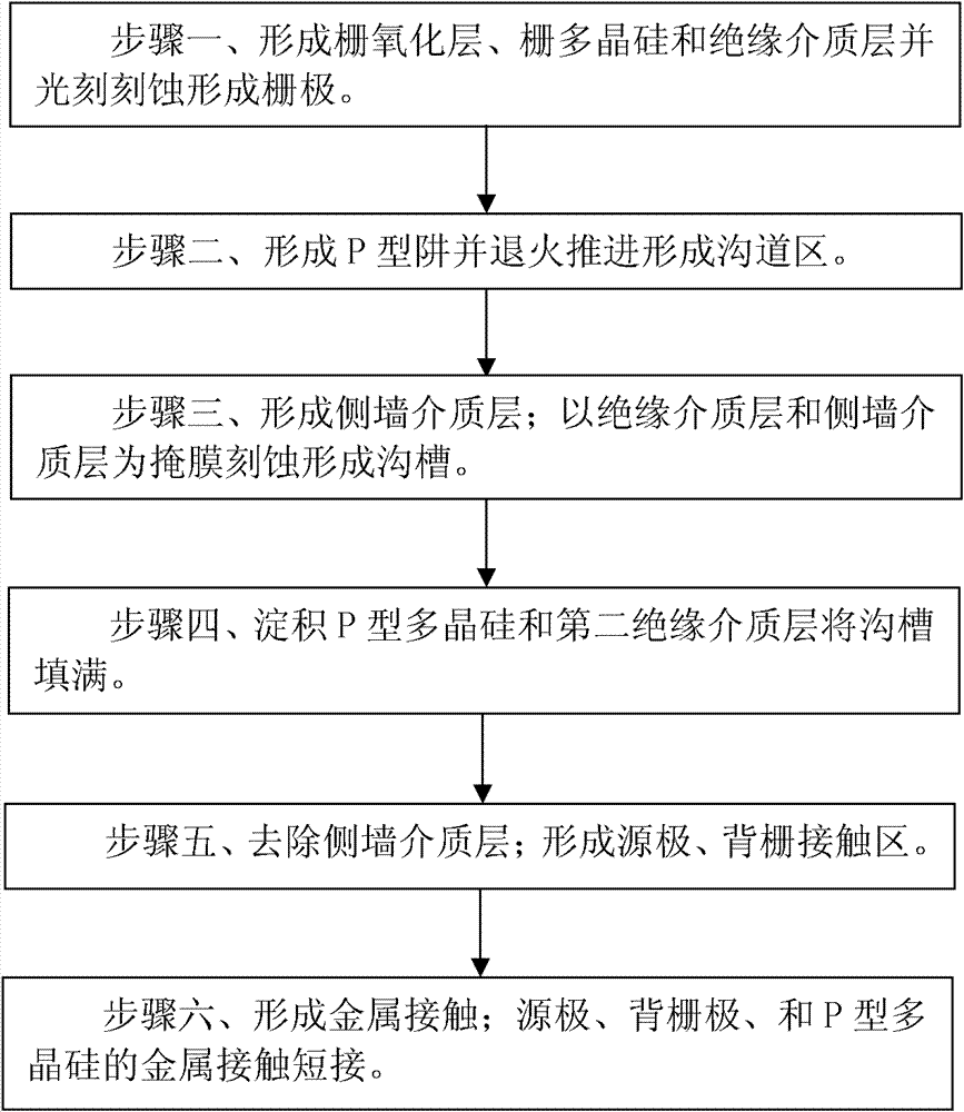
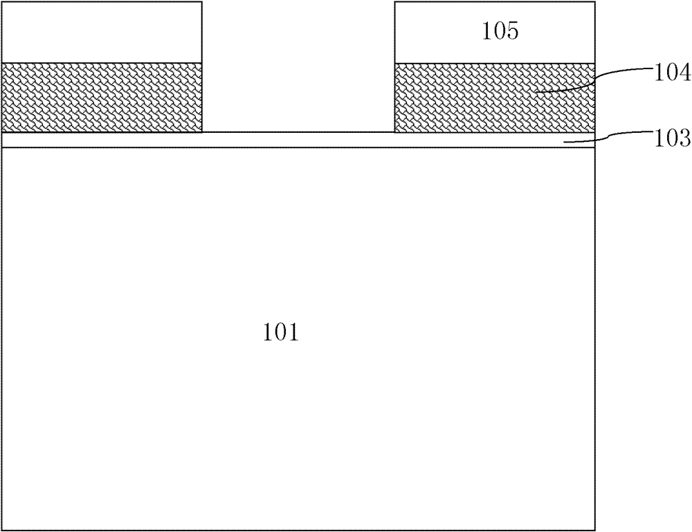
[0023] like figure 1 Shown is the flow chart of the method of the embodiment of the present invention; Figure 2 to Figure 7 Shown is a schematic diagram of the device structure in each step of the method of the embodiment of the present invention. The manufacturing method of the power transistor according to the embodiment of the present invention includes the following steps:

[0024] Step one, such as figure 2 As shown, a gate oxide layer 103, a gate polysilicon 104 and an insulating dielectric layer 105 are sequentially formed on the surface of the N-type pressure receiving region 101 from bottom to top; the insulating dielectric layer 105 and the gate polysilicon 104 are etched performing etching to form the gate.

[0025] The isolated power transistor can be a silicon-based device or a compound semiconductor device. When the isolated power transistor is a silicon-based device, the N-type pressure receiving region 101 is a silicon epitaxial layer, or Czochralski sing...


PUM

PropertyMeasurementUnit
thicknessaaaaaaaaaa
thicknessaaaaaaaaaa

Abstract

The invention discloses a method for manufacturing a power transistor. By the method, insulating dielectric layers formed on the top of grid polycrystalline silicon and side-wall dielectric layers formed on side surfaces of the insulating dielectric layers are used as etching hard masks of a pressure bearing region, the quantity of masks required by a front-surface process is reduced, and the density of a transistor in a chip can be increased. A P-type polycrystalline silicon layer is planted into a P-type well region and is subjected to short circuit with a source electrode via metal contact, cavity flows of the P-type well region flow out advantageously, and accumulated cavities are reduced, so that latch-up resistance of a device is improved. The method is favorable for obtaining a power device with low conducting resistance, low saturation voltage drop and high current driving capacity.

Description

technical field [0001] The invention relates to a semiconductor integrated circuit manufacturing process method, in particular to a power transistor manufacturing method. Background technique [0002] In the application of power and high-voltage devices, it is hoped that the on-resistance of the transistor will be smaller, the saturation voltage drop will be lower, and the current driving capability will be greater. How to integrate more devices within a certain chip area is particularly important. However, the alignment deviation between different masks makes the device size unable to be reduced according to the demand, and the more precise photolithography technology makes the manufacturing cost expensive, which is not conducive to mass production. In addition, when the hole current in the well region reaches a certain level, the potential of the well region will be raised, and the source-well junction barrier will be lowered, causing the parasitic bipolar transistor to be...

Claims


Application Information

Patent Timeline
Patent Type & Authority Applications(China)
IPC IPC(8): H01L21/336H01L21/331
Inventor 韩峰段文婷
Owner SHANGHAI HUAHONG GRACE SEMICON MFG CORP
Why Eureka
Try Eureka