Manufacturing method of groove-type superjunction device

A manufacturing method and super-junction technology, applied in semiconductor/solid-state device manufacturing, semiconductor devices, electrical components, etc., can solve problems such as deep and wide, low performance of pitch on-resistance, and poor wafer uniformity, and achieve improved Effects of reverse breakdown voltage, improved in-plane uniformity, reduced width and pitch

Active Publication Date: 2015-07-15
SHANGHAI HUAHONG GRACE SEMICON MFG CORP
View PDF5 Cites 17 Cited by
  • Summary
  • Abstract
  • Description
  • Claims
  • Application Information

AI Technical Summary

Problems solved by technology

Since the actual difference between Top CD and Bottom CD is too large, it is difficult for the super junction to achieve charge balance at the top and bottom of the trench 104 at the same time, which seriously affects the reverse breakdown voltage of the device.
[0004] In addition, when making super junction devices through deep trench technology, the deep trench has a large aspect ratio, and when the trench is deep, the process difficulty of deep trench etching and epitaxial layer (EPI) filling is greatly increased.
When the deep trench is deep, the uniformity of the in-plane depth of the wafer (wafer) becomes poor, and the time and difficulty of epitaxial filling (EPI Filling) increase significantly, which has a great impact on equipment capability and production capacity
[0005] It is precisely because of these limitations that it is difficult to manufacture devices with further reduced pitch (Pitch), lower on-resistance (RSP) and better performance by using the existing deep trench process method, and it is also difficult to manufacture devices with a reverse breakdown voltage above 800V super junction device

Method used


Image

  • Manufacturing method of groove-type superjunction device
  • Manufacturing method of groove-type superjunction device
  • Manufacturing method of groove-type superjunction device

Examples


Embodiment Construction

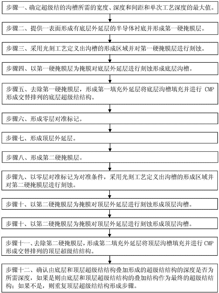
[0042] Such as figure 2 Shown is the flow chart of the method of the embodiment of the present invention; Figure 3A to Figure 3H Shown is a schematic diagram of the device structure in each step of the method of the embodiment of the present invention. The manufacturing method of the trench type super junction device according to the embodiment of the present invention includes the following steps:

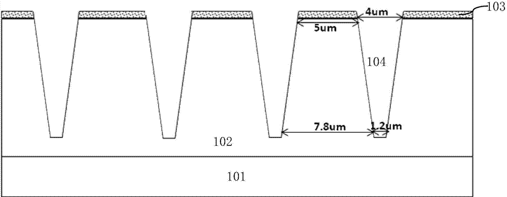
[0043] Step 1. Determine the required width, depth and spacing of the grooves of the super junction according to the reverse breakdown voltage and on-resistance requirements of the trench-type super junction device; according to the equipment and process capabilities of the production line and the required The width of the trench determines the maximum value of the single process depth corresponding to the width of the trench required for one photolithography etching and filling process, and the maximum value of the single process depth requires that the The difference between...


PUM


Abstract

The invention discloses a manufacturing method of a groove-type superjunction device. The manufacturing method comprises the following steps as follows: determining groove size parameters and the maximum value of a single-process depth; providing a substrate, and forming a first hard mask layer; defining a groove forming region; etching a bottom epitaxial layer to form a bottom groove; removing the first hard mask layer, epitaxially filling the bottom groove, and performing CMP; forming a zero layer aligning mark; forming a top epitaxial layer; forming a second hard mask layer; with the zero layer aligning mark as a aligning condition, defining the groove forming region; etching the top epitaxial layer to form a top groove; removing the second hard mask layer, epitaxially filling the top groove, and performing CMP; checking whether the depth of a laminated superjunction structure reaches a required depth, if so, ending the manufacturing method, otherwise, repeating the top superjunction structure forming step. By the manufacturing method, reverse breakdown voltage of a superjunction device can be increased, the conduction resistance can be reduced, the existing equipment and the existing process can be utilized to the maximum extent.

Description

technical field [0001] The invention relates to a manufacturing process method of a semiconductor integrated circuit, in particular to a manufacturing method of a trench type super junction device. Background technique [0002] When fabricating super junction devices by deep trench (trench) process, the morphology of deep trench is very important. However, due to the limitations of the etching process, the generally obtainable deep trenches have poor morphology and small sidewall angles. When the trench is shallow, the effect is small, but when the trench width, that is, the corresponding characteristic dimension (CD, Critical Dimension) is as small as less than 5 μm and the depth reaches more than 40 μm, the top width (Top CD) and the bottom width (Bottom CD) will vary greatly. It is very unfavorable to increase the reverse breakdown voltage of the device. Such as figure 1 Shown is a schematic structural diagram of a trench-type superjunction device formed by an existin...

Claims


Application Information

Patent Timeline
Patent Type & Authority Applications(China)
IPC IPC(8): H01L29/78H01L21/336H01L29/06
CPCH01L29/06H01L29/0611H01L29/66477H01L29/78
Inventor 徐向明李昊
Owner SHANGHAI HUAHONG GRACE SEMICON MFG CORP
Why Eureka
Try Eureka