Method for Embedding Capacitor in Printed Circuit Board and Printed Circuit Board
A technology of printed circuit boards and embedded capacitors, which is applied in the direction of printed circuits connected with non-printed electrical components, multi-layer circuit manufacturing, and printed circuits assembled with electrical components. It can solve the problem of screen printing plane size and thickness uniformity control Poor, poor capacitance accuracy, difficult to control and other issues, to achieve the effect of improving signal integrity, reducing mounting costs, and reducing the size of the board
- Summary
- Abstract
- Description
- Claims
- Application Information
AI Technical Summary
Problems solved by technology
Method used
Image
Examples
Embodiment 1
[0043] (1) Substrate production:
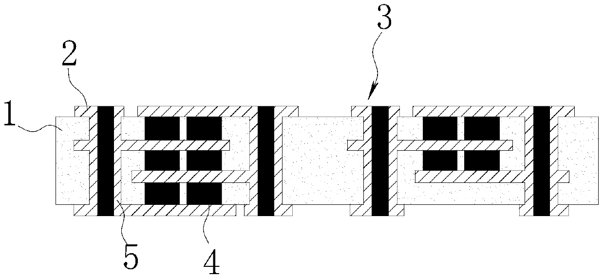
[0044] (a) Production of matrix 1: 1) The insulation material is cut, the resin in the insulation material is not fully cured, and is in a semi-cured state. The resin in the insulation material can be epoxy resin, phenolic resin or BT resin, etc., and the insulation material can contain Inorganic filler, reinforcement layer, etc., the reinforcement layer is preferably glass fiber cloth; 2) Paste the protective film, the bonding temperature is between 60°C and 150°C, the bonding temperature must be below the glass transition temperature of the insulating material, the protective film can It is polyester film, polyimide film, etc., and its thickness is between 5 μm and 100 μm; 3) Drilling, the drilling is a through hole, that is, the through hole runs through the upper and lower sides of the board, and the drilling can be done by mechanical drilling, It can be realized by laser drilling or punching. Laser drilling can be realized by infrared la...
Embodiment 2
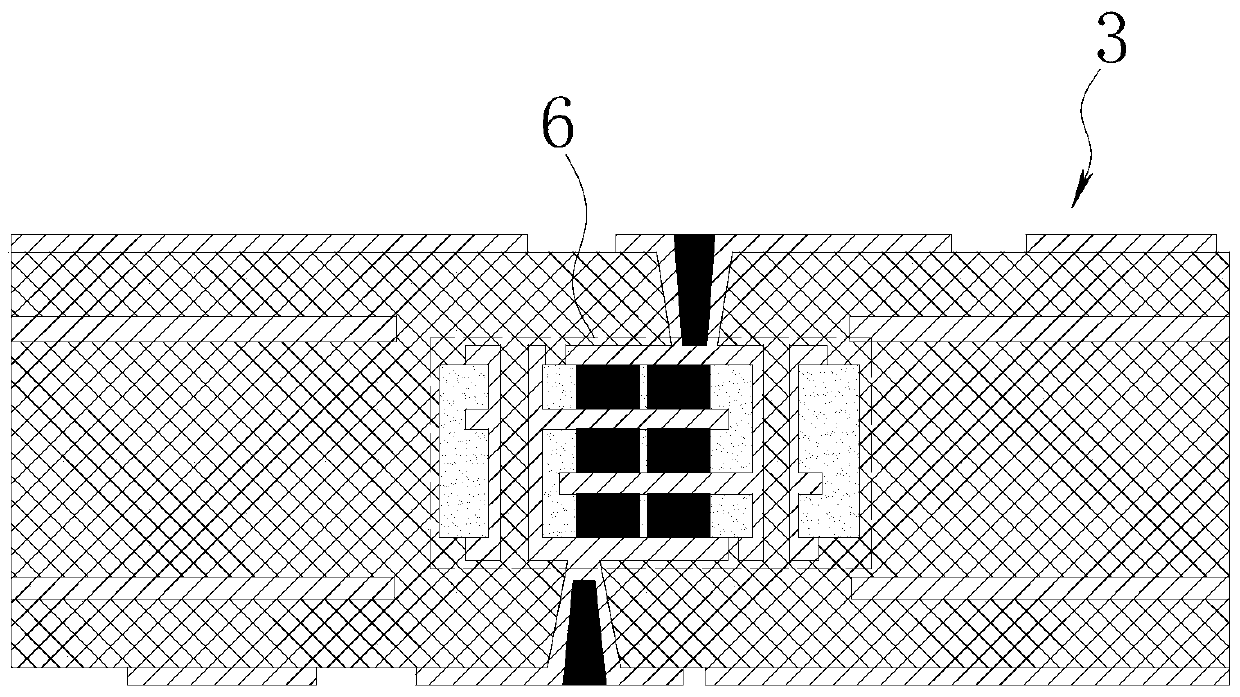
[0051] A method for embedding capacitors in a printed circuit board of the present invention, its process is basically the same as that of Embodiment 1, the difference is that the preparation method of the base body 2 and the base body 3 and the way of stacking the plates during pressing are different in this embodiment .
[0052] The preparation method of the substrate 2 is specifically as follows: 1) Cutting the printed circuit board. The printed circuit board can be an insulating substrate, single-layer, double-layer or multi-layer board. The printed circuit board includes an insulating material and a metal layer. The resin has been completely cured. The resin in the insulating material can be epoxy resin, phenolic resin or BT resin. The insulating material can contain inorganic fillers, reinforcing layers, etc. The reinforcing layer is preferably glass fiber cloth. The metal layer can be made of copper, silver, etc. layer, gold layer, etc., preferably copper layer; 2) dril...
PUM
 Abstract
Description
Claims
Application Information

