Preparation method of TEM sample

A sample and target structure technology, applied in the field of semiconductor manufacturing, can solve the problems of difficult to prepare MEMS samples with suspended films, difficult to achieve MEMS sample filling, and difficult to ensure the consistency of target structures, etc., to save preparation time, reduce damage, Simple and easy method

Active Publication Date: 2015-07-22
SEMICON MFG INT (SHANGHAI) CORP
View PDF17 Cites 14 Cited by
  • Summary
  • Abstract
  • Description
  • Claims
  • Application Information

AI Technical Summary

Problems solved by technology

[0011] In view of the above-mentioned shortcoming of prior art, the purpose of the present invention is to provide a kind of preparation method of TEM sample, is used to solve the problem that the existing TEM sample preparation technology is difficult to prepare the MEMS sample with suspending film, promptly is used to solve the problem that adopts Before preparing TEM samples by conventional methods, it is very difficult to fill MEMS samples with a suspended film structure. When MEMS samples are prepared directly using conventional TEM sample preparation methods without filling the suspended film structure, the FIB preparation process of the sample In the middle, the high-energy ion beam will cause damage to the suspended film, it is difficult to ensure the integrity of the sample during the entire sample preparation process, which greatly affects the accuracy of the sample observation results, and the separation of the MEMS suspended film from the substrate Then transfer it to the Si blank, and then use the existing preparation process to prepare the TEM sample, the suspended film must be transferred by ectopic absorption, so it is difficult to ensure the angle of the target structure taken out and the angle in the matrix problem of consistency

Method used


Image

  • Preparation method of TEM sample
  • Preparation method of TEM sample
  • Preparation method of TEM sample

Examples


Embodiment Construction

[0047] Embodiments of the present invention are described below through specific examples, and those skilled in the art can easily understand other advantages and effects of the present invention from the content disclosed in this specification. The present invention can also be implemented or applied through other different specific implementation modes, and various modifications or changes can be made to the details in this specification based on different viewpoints and applications without departing from the spirit of the present invention.

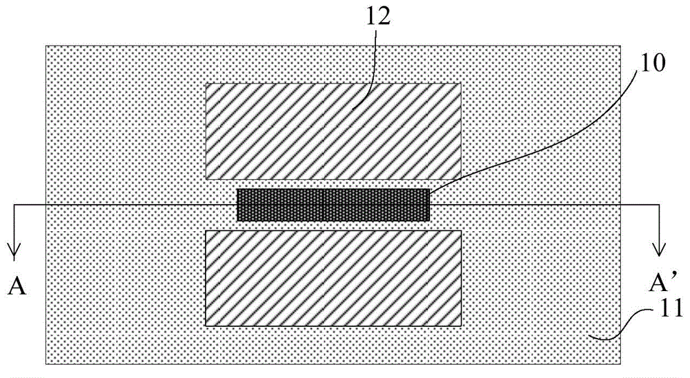
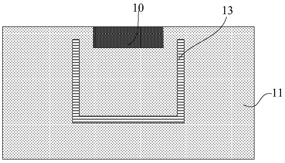
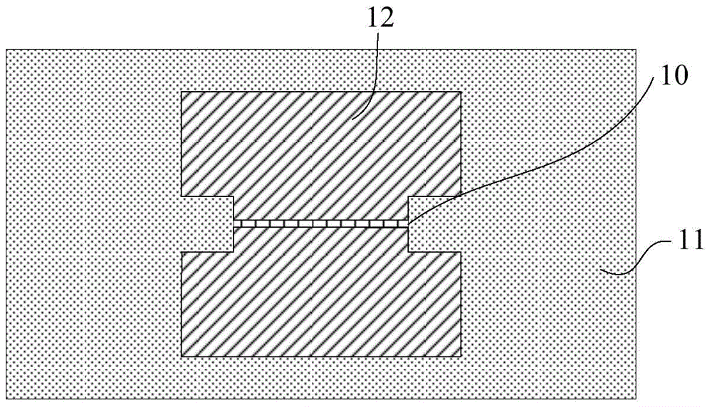
[0048] see Figure 2 to Figure 3f It should be noted that the illustrations provided in this embodiment are only schematically illustrating the basic idea of ​​the present invention, although only the components related to the present invention are shown in the drawings rather than the number and shape of components in actual implementation and size drawing, the type, quantity and proportion of each component can be changed arbitraril...


PUM

PropertyMeasurementUnit
thicknessaaaaaaaaaa

Abstract

The invention provides a preparation method of a TEM sample. According to the preparation method, low-current L-shape or U-shape cutting is firstly carried out on a target structure in a suspended film structure at the top of an MEMS sample by the use of a low-energy ion beam; then, the target structure is cut off from the suspended film structure through adhering by a probe of a nano-manipulation instrument; and finally, the target structure is transferred onto a copper bracket by an in situ adsorption mode to undergo fine-polishing and thinning. According to the invention, damage to the target structure is reduced to the maximum and integrity of a sample is guaranteed to the maximum during the whole sample preparation process; consistency of angle of the target structure when taken out with angle of the target structure in the suspended film structure is guaranteed, and observation result accuracy of the target structure is greatly enhanced; and in comparison with an existing TEM sample preparation process of MEMS by firstly transferring a suspended film onto a Si sheet and then preparing a sample, the method provided by the invention is simple and easy to operate so as to save preparation time of samples.

Description

technical field [0001] The invention relates to the technical field of semiconductor manufacturing, in particular to the field of TEM sample preparation methods. Background technique [0002] TEM (Transmission Electron Microscope, Transmission Electron Microscope) is a very important tool used in the semiconductor manufacturing industry to detect the shape, size and characteristics of the thin films that make up the device. It uses high-energy electron beams as light sources and electromagnetic fields as lenses. The accelerated and focused electron beam is projected onto a very thin sample, and the electrons and atoms in the sample change direction due to collisions, resulting in solid angle scattering. The size of the scattering angle is related to the density and thickness of the sample, so images with different light and dark can be formed. One of the outstanding advantages of TEM is that it has high resolution and can observe the shape and size of extremely thin films. ...

Claims


Application Information

Patent Timeline
Patent Type & Authority Applications(China)
IPC IPC(8): G01N1/28
Inventor 齐瑞娟于会生
Owner SEMICON MFG INT (SHANGHAI) CORP
Why Eureka
Try Eureka