Wafer packaging structure, chip packaging structure and packaging method thereof

A wafer packaging and wafer technology, applied in radiation control devices, electrical components, electrical solid devices, etc., can solve the problems of affecting the etching process, bulging, and generating flyers, etc.

Active Publication Date: 2015-07-22
HUATIAN TECH KUNSHAN ELECTRONICS
View PDF6 Cites 5 Cited by
  • Summary
  • Abstract
  • Description
  • Claims
  • Application Information

AI Technical Summary

Problems solved by technology

When electrostatic adsorption is implemented, an electrostatic film will be pasted on the first surface of the substrate, but for a substrate with a groove formed on the first surface of the substrate, the electrostatic film will cover the groove to form a closed space with air, so that

Method used


Image

  • Wafer packaging structure, chip packaging structure and packaging method thereof
  • Wafer packaging structure, chip packaging structure and packaging method thereof
  • Wafer packaging structure, chip packaging structure and packaging method thereof

Examples


Embodiment 1

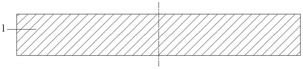
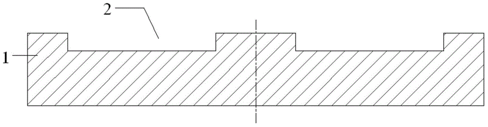
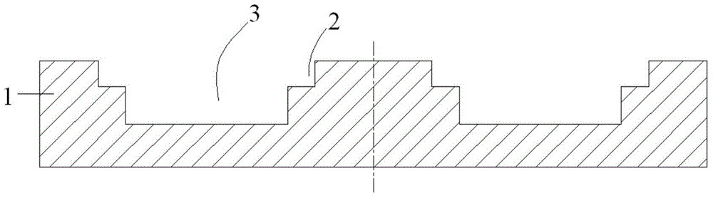
[0055] see Figure 11 , Figure 12 , Figure 13 with Figure 14 , a wafer packaging structure, including a large base with several base units 1 and a wafer with several image sensor chip units 9 .

[0056] The large substrate has a first surface and a second surface opposite to it. At least one first groove 2 is formed in the middle of the first surface of each base unit, and at least one exhaust gas is formed around the first groove of the middle base unit. Groove 4, the exhaust groove communicates with the first groove of the peripheral adjacent base unit, at least one exhaust groove is formed on the periphery of the first groove of the base unit on the edge, and the exhaust groove extends to the edge of the substrate Connect with the external environment. better, see Figure 12 , the four sides of the first groove 2 of each base unit are respectively provided with an exhaust groove 4, and the four exhaust grooves all extend to the outside of the edge of the base unit, ...

Embodiment 2

[0080] see Figure 16 with Figure 17 , a wafer package structure, comprising a large base with several base units 1, the large base has a first surface and a second surface opposite to it, at least one first groove is formed in the middle of the first surface of each base unit 2. At least one exhaust groove 4 is formed on the periphery of the first groove of the middle base unit. There is at least one exhaust groove, and the exhaust groove extends to the edge of the base to communicate with the external environment. Preferably, the four sides of the first groove 2 of each base unit are respectively provided with an exhaust groove 4, and the four exhaust grooves all extend to the outside of the edge of the base unit, that is, between the horizontal plane below the first surface of the base and The external environment is connected.

[0081] The bottom of the first groove is provided with a functional chip 12, the functional chip has a first surface and a second surface oppo...


PUM


Abstract

The invention discloses a wafer packaging structure, a chip packaging structure and a packaging method thereof. The wafer packaging structure comprises a large substrate with a plurality of substrate units; the large substrate comprises a first surface and an opposite second surface, the middle of the first surface of each substrate unit is provided with at least one first groove, at least one exhausting groove is formed in the middle of the substrate unit surrounding the first groove and is communicated with the first groove communicated with the adjacent surrounding substrate units, and at least one exhaust groove is formed in the substrate unit of the edge surrounding the first groove and extends to the edge of the substrate to communicate with the outside. Thus, the first groove of the large substrate can be communicated with a cavity, the air pressure of the cavity and first groove can be balanced, a static film is prevented from plumping during evacuation, and the film electrostatic adsorption capacity in the dry etching process is guaranteed; the chip packaging structure is obtained by cutting and segmenting the wafer packaging structure.

Description

technical field [0001] The invention relates to the technical field of wafer level packaging, in particular to a wafer packaging structure, a chip packaging structure and a packaging method thereof. Background technique [0002] In the wafer packaging structure, the substrate is used as a carrier or support for other chips, and usually has an opposite first surface and a second surface. In some wafer packaging processes, it is usually necessary to perform dry etching on the second surface of the substrate to form openings. Or carry out dry etching to the non-functional surface of the wafer bonded to the second surface of the substrate to form openings, and when performing dry etching to form openings, it is necessary to first adsorb the first surface of the substrate by means of electrostatic adsorption and other methods. Positioning is performed, and then an etching process is performed in a vacuum environment. When electrostatic adsorption is implemented, an electrostatic...

Claims


Application Information

Patent Timeline
IPC IPC(8): H01L29/06H01L27/146
CPCH01L23/12H01L27/146H01L27/14687H01L29/0657
Inventor 万里兮范俊黄小花翟玲玲钱静娴项敏马力
Owner HUATIAN TECH KUNSHAN ELECTRONICS
Why Eureka
Try Eureka