Film bulk acoustic resonator and preparation method thereof

A thin-film bulk acoustic wave and resonator technology, which is applied in the direction of electrical components, impedance networks, etc., can solve the problems of difficulty in consistent etching rates and bulges, and achieve the effect of solving differences

Pending Publication Date: 2020-04-28
广州市艾佛光通科技有限公司
View PDF0 Cites 8 Cited by
  • Summary
  • Abstract
  • Description
  • Claims
  • Application Information

AI Technical Summary

Problems solved by technology

However, in practice, the etching rate is difficult to be consistent across the entire plane, and the thinner silicon binding force becomes smaller, and different degrees of bulges or depressions will appear during the silicon removal process.

Method used


Image

  • Film bulk acoustic resonator and preparation method thereof
  • Film bulk acoustic resonator and preparation method thereof
  • Film bulk acoustic resonator and preparation method thereof

Examples


Embodiment 1

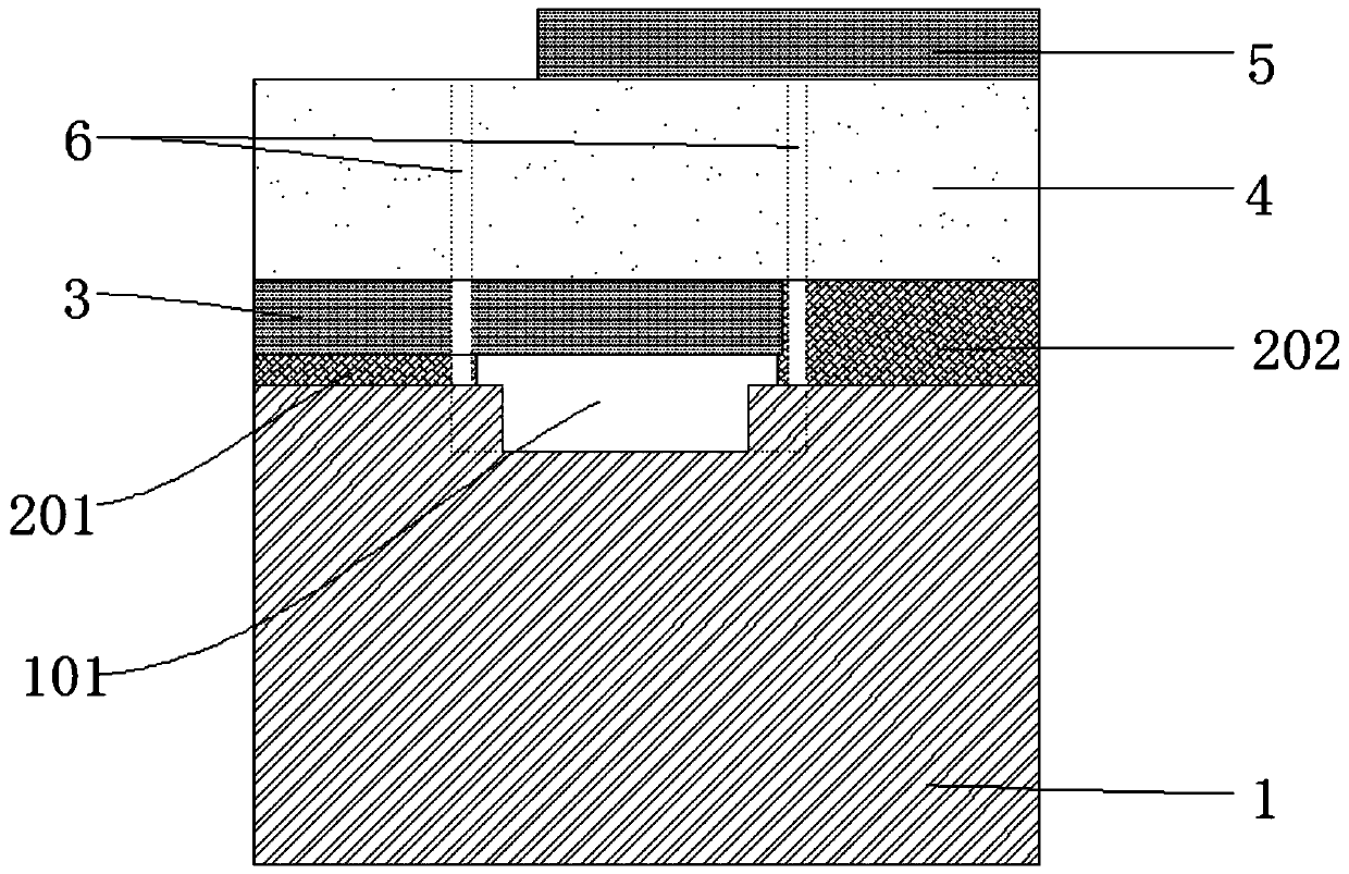
[0056] Such as Figure 1~3 As shown, a thin film bulk acoustic resonator includes a substrate, and the substrate is set as a silicon substrate, that is, a silicon wafer 1, wherein the silicon adopts high-resistance silicon with a resistivity greater than 10000Ω to avoid substrate coupling Part of the energy affects the insertion loss and signal.

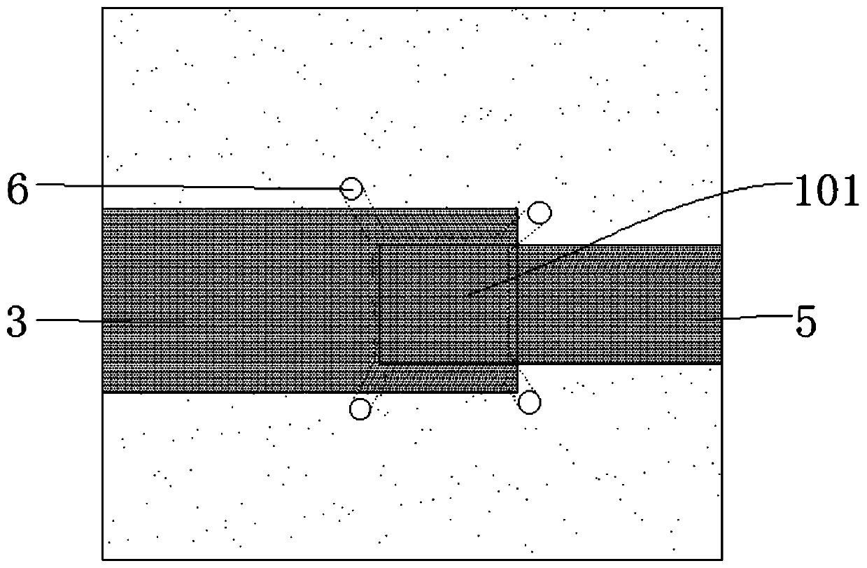
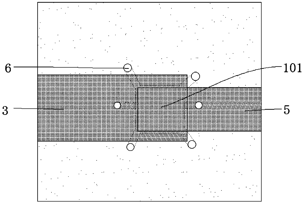
[0057]And a cavity 101 is opened on the substrate, the depth of the cavity 101 is between 2um~4um, and in this embodiment, the cavity depth of the cavity 101 is about 3um, because it does not involve filling , so the inner wall of the cavity 101 and the bottom surface of the cavity 101 can be made into a vertical angle; and the communication channel of the cavity 101, considering the structural stability and process requirements, preferably, can be 10-20um between. In addition, the number of the through-holes 6 communicating with the cavity 101 is set at least two, which can prevent the air in the cavity 101 from being blocked by o...

Embodiment 2

[0066] A method for preparing a thin film bulk acoustic resonator, used to prepare the thin film bulk acoustic resonator as in Example 1, such as Figure 4a~Figure 4m shown, including the following steps:

[0067] Step S1: Select a silicon wafer 1, and engrave a cavity 101 on the silicon wafer 1, such as Figure 4a .

[0068] First select a silicon wafer 1, mark the silicon wafer 1 to facilitate subsequent identification and registration; and pickle and organically wash it to remove impurities such as oxides and organic substances on the silicon wafer 1 . Thereafter, the silicon wafer 1 is uniformly coated, exposed, and developed, and then placed in an ICP device for cavity carving, and a patterned substrate with a cavity 101 is formed after the glue is removed.

[0069] Step S2: growing a bonding layer 2 on the silicon wafer 1 outside the cavity 101, such as Figure 4b .

[0070] The bonding layer 2 also needs to be patterned using an exposure machine. If the bonding lay...

Embodiment 3

[0087] This embodiment is improved on the basis of Embodiment 2. In this embodiment, the bonding layer 2 is metal bonding, and the steps S1 to S4 are the same as those described in Embodiment 2. After the step S4, a step S41 is also included: a support layer 9 is grown on the upper surfaces of the bottom electrode layer 3 and the bonding layer 2, and the support layer 9 can completely cover the bottom electrode layer 3 and the The upper surface of bonding layer 2, such as Figure 6 shown; it can also grow behind the bottom electrode layer 3 and the upper surface of the bonding layer 2, and leave a gap at the position corresponding to the cavity 101, as Figure 5 shown. The thickness of the support layer 9 is preferably above 1um. The material of the supporting layer 9 can be a traditional supporting material, such as silicon nitride.

[0088] Thereafter, the bonding layer 2 in step S5 can be directly grown on the upper surface of the support layer 9 , and the subsequent ste...


PUM


Abstract

The invention discloses a film bulk acoustic resonator and a preparation method thereof, and the resonator comprises a substrate which is provided with a cavity; a bonding layer which comprises a first bonding layer and a second bonding layer which are arranged on the upper surface of the substrate outside the cavity, wherein the thickness of the first bonding layer is less than that of the secondbonding layer; a bottom electrode layer which is arranged on the upper surface of the first bonding layer and completely covers the cavity, so the bottom electrode layer is flush with the second bonding layer; a piezoelectric layer which is arranged on the upper surfaces of the bottom electrode layer and the second bonding layer, wherein a through hole is formed in the piezoelectric layer and penetrates through the piezoelectric layer, and the bottom electrode layer and the bonding layer to be communicated with the cavity; a top electrode layer which is arranged on the upper surface of the piezoelectric layer, wherein the orthographic projections of the top electrode layer and the bottom electrode layer on the horizontal plane only coincide at the positions corresponding to the cavities.According to the preparation method, before silicon is completely removed, the cavity is communicated with the outside, and the difference between the interior of the cavity and the atmospheric pressure is solved under the condition that silicon binding force with enough strength exists.

Description

technical field [0001] The invention relates to the field of acoustic wave resonators, in particular to a film bulk acoustic wave resonator and a preparation method thereof. Background technique [0002] At present, in the commercial traditional FBAR manufacturing technology, there are mainly two categories. One is that the outermost interface of the FBAR core functional area is in contact with the air interface to form a sound wave total reflection surface to ensure the effective realization of the FBAR function; the other is The cavity is not carved on the silicon substrate, but a layer structure with alternating low acoustic impedance and high acoustic impedance is grown to form a sound transmission reflection surface. [0003] These two technologies have been developed relatively maturely. For the formation of the sound transmission reflection surface, it is mainly realized by the air interface, and the effect is better. For the formation of such an air surface, it can b...

Claims


Application Information

Patent Timeline
Patent Type & Authority Applications(China)
IPC IPC(8): H03H3/02H03H9/17
CPCH03H3/02H03H9/171
Inventor 李国强
Owner 广州市艾佛光通科技有限公司
Why Eureka
Try Eureka