Supercharge Your Innovation With Domain-Expert AI Agents!

SA-LIGBT (shorted-anode lateral insulated gate bipolar transistor) capable of restraining snapback effect

A negative resistance effect and substrate technology, applied in the field of SA-LIGBT, can solve problems such as practical production difficulties, inconvenient practical applications, adverse effects on device reliability and stability, etc., and achieve the effect of suppressing snapback phenomenon and excellent snapback phenomenon

Inactive Publication Date: 2015-07-22
UNIV OF ELECTRONICS SCI & TECH OF CHINA
View PDF5 Cites 7 Cited by
  • Summary
  • Abstract
  • Description
  • Claims
  • Application Information

AI Technical Summary

Problems solved by technology

However, this traditional SA-LIGBT will have a negative resistance effect (snapback) during forward conduction, which will prevent the complete conduction of the SA-LIGBT, which will adversely affect the reliability and stability of the device.
In order to suppress the negative resistance effect, Byeong-Hoon Lee et al. proposed GHI-LIGBT (Gradual Hole Injection Dule-gate LIGBT), such as figure 2 As shown, compared with the traditional SA-LIGBT, the GHI-LIGBT introduces a second gate next to the N collector region, and forms a P between the field oxygen and the second gate by ion implantation + Layer, when the device is forward-conducting, the first gate is positively biased, the second gate is negatively biased, the N+ emitter and the P+ collector emit electrons and holes respectively at the same time, and the P+ layer can assist in enhancing the flow of holes. Emission efficiency makes GHI-LIGBT work in bipolar conduction mode, thereby suppressing the negative resistance effect, but this structure is a four-terminal device, which is inconvenient in practical applications
In order to suppress the negative resistance effect while ensuring that the device is still a three-terminal device, Juhyun Oh et al. proposed a SA-LIGBT with a trench collector, such as image 3 As shown, compared with the traditional SA-LIGBT, this structure increases the resistance of the N-type buffer layer under the P-type collector region through which the electron current flows through the trench structure of the collector region, so that the P-type collector region / N-type The buffer layer junction is easier to conduct, thus suppressing the negative resistance effect, but this structure needs to dig grooves, fill dielectric layers, etc. in the process, and the process complexity is relatively large, which brings difficulties to actual production

Method used


Image

  • SA-LIGBT (shorted-anode lateral insulated gate bipolar transistor) capable of restraining snapback effect
  • SA-LIGBT (shorted-anode lateral insulated gate bipolar transistor) capable of restraining snapback effect
  • SA-LIGBT (shorted-anode lateral insulated gate bipolar transistor) capable of restraining snapback effect

Examples


Embodiment Construction

[0019] The present invention is described in detail below in conjunction with accompanying drawing

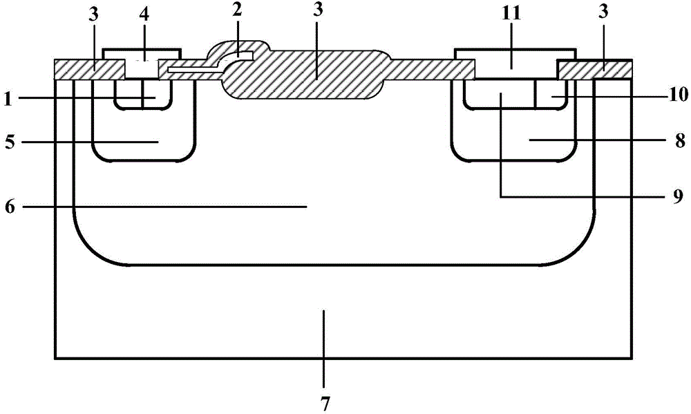
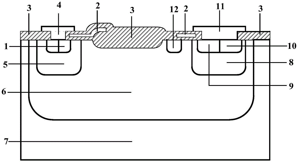
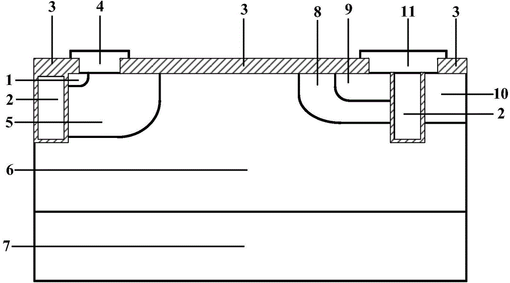
[0020] A new SA-LIGBT structure that eliminates the negative resistance effect proposed by the present invention is based on the traditional SA-LIGBT, through the etching process of the anode metal, the electrode contact between the P-type collector area and the N-type collector area A metal resistor of appropriate resistance is produced between them. When the device is forward-conducting (anode plus high voltage), the current flows through the metal resistance and generates a voltage drop on it, so that a voltage difference is generated between the P-type collector area / N-type buffer layer junction, so that the PN junction is forward-conducting It prevents the MOS part inside the device from being turned on before the IGBT part and the negative resistance phenomenon occurs. It is worth noting that using this method, the snapback phenomenon can be well suppressed without incre...


PUM

PropertyMeasurementUnit
Resistanceaaaaaaaaaa

Abstract

The invention relates to the power semiconductor technology, in particular to an SA-LIGBT (shorted-anode lateral insulated gate bipolar transistor) capable of restraining a snapback effect. An implementing method for the SA-LIGBT mainly includes that a metal resistor with a certain resistance value is generated between electrode contacts of a P-type collecting region and an N-type collecting region, and the resistance value of the metal resistor can be controlled by adjusting the area and the length of the metal resistor. When a device is turned on forwardly, current IF flows through the metal resistor R and generates a voltage drop IFR on the metal resistor to generate voltage difference between the P-type collecting region and an N-type buffering layer, if the IFR is larger than a forward turn-on voltage drop of a PN junction, the PN junction is turned on forwardly and enters an IGBT (insulated gate bipolar transistor) working mode, and thus, the snapback effect is restrained effectively. The SA-LIGBT has the advantages that capability of effectively restraining a snapback phenomenon without increasing technical complexity excessively, and other performance parameters of the SA-LIGBT cannot be affected.

Description

technical field [0001] The invention relates to power semiconductor technology, in particular to a SA-LIGBT (Shorted-Anode Lateral Insulated Gate Bipolar Transistor, Shorted-Anode Lateral Insulated Gate Bipolar Transistor) capable of suppressing the negative resistance effect. Background technique [0002] Lateral Insulated Gate Bipolar Transistor (LIGBT) is a new type of component in power integrated circuits. It not only has the advantages of easy driving and simple control of LDMOSFET, but also has the advantages of low turn-on voltage of power transistors, large on-state current, and low loss. It has become one of the core components of modern power semiconductor integrated circuits. Literature (Shigeki T., Akio N., Youichi A., Satoshi S. and Norihito T. Carrier-Storage Effect and Extraction-Enhanced Lateral IGBT (E 2 LIGBT): A Super-High Speed ​​and Low On-state Voltage LIGBT Superior to LDMOSFET.Proceedings of 2012International Symposium on Power Semiconductor Devices...

Claims


Application Information

Patent Timeline
IPC IPC(8): H01L29/739H01L21/331H01L21/28
CPCH01L21/28H01L29/401H01L29/41708H01L29/66325H01L29/7393
Inventor 任敏刘永杨珏琳蔡果牛博伍济朱章丹陈海文李泽宏张波
Owner UNIV OF ELECTRONICS SCI & TECH OF CHINA
Features
  • R&D
  • Intellectual Property
  • Life Sciences
  • Materials
  • Tech Scout
  • Unparalleled Data Quality
  • Higher Quality Content
  • 60% Fewer Hallucinations
Learn More