Supercharge Your Innovation With Domain-Expert AI Agents!

A SiC Junction Barrier Schottky Diode Device with Ladder Termination

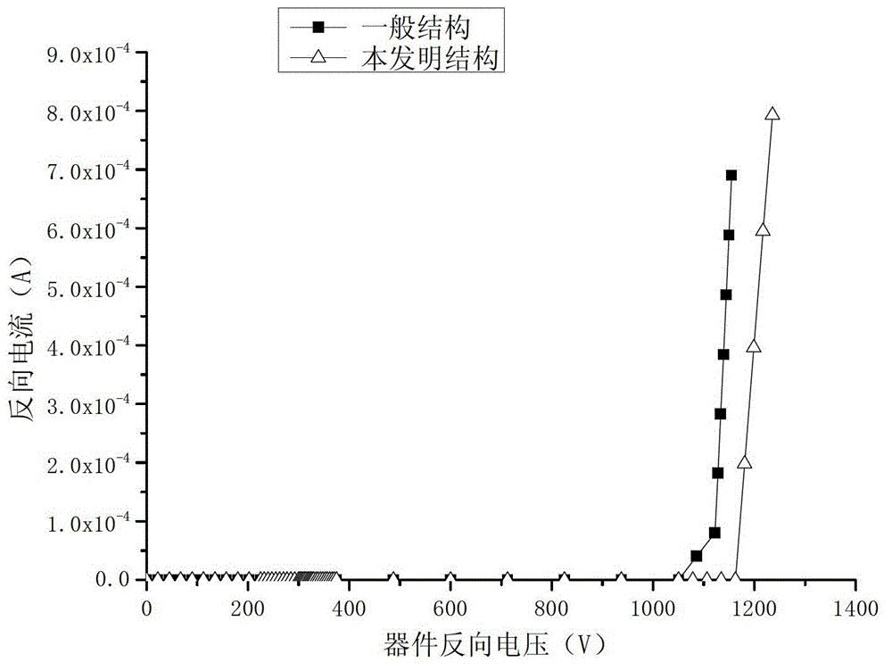
A technology of junction barrier Schottky and silicon carbide, applied in the direction of semiconductor devices, electrical components, circuits, etc., can solve the problems of increasing the forward voltage drop and increasing the forward conduction resistance of the device, so as to reduce the local high field and improve the Inverse characteristic curve, effect of high withstand voltage

Active Publication Date: 2015-10-07
SOUTHEAST UNIV
View PDF5 Cites 0 Cited by
  • Summary
  • Abstract
  • Description
  • Claims
  • Application Information

AI Technical Summary

Problems solved by technology

One way to improve the withstand voltage of power devices is to increase the thickness of the low-doped epitaxial layer, but this will increase the forward conduction resistance of the device, thereby increasing the forward voltage drop

Method used


Image

  • A SiC Junction Barrier Schottky Diode Device with Ladder Termination
  • A SiC Junction Barrier Schottky Diode Device with Ladder Termination
  • A SiC Junction Barrier Schottky Diode Device with Ladder Termination

Examples


Embodiment Construction

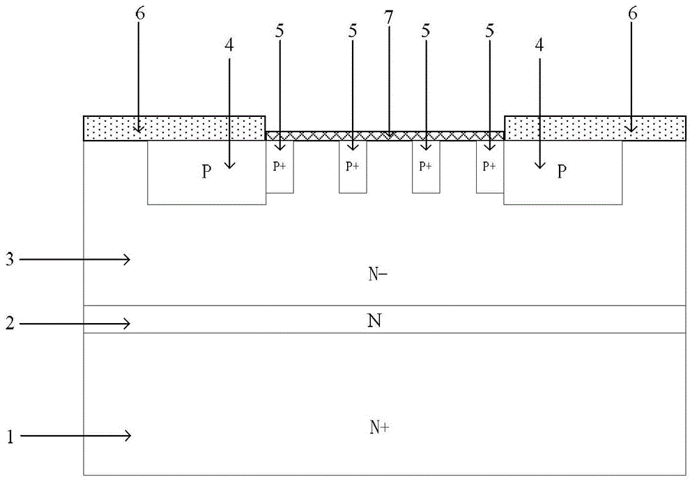
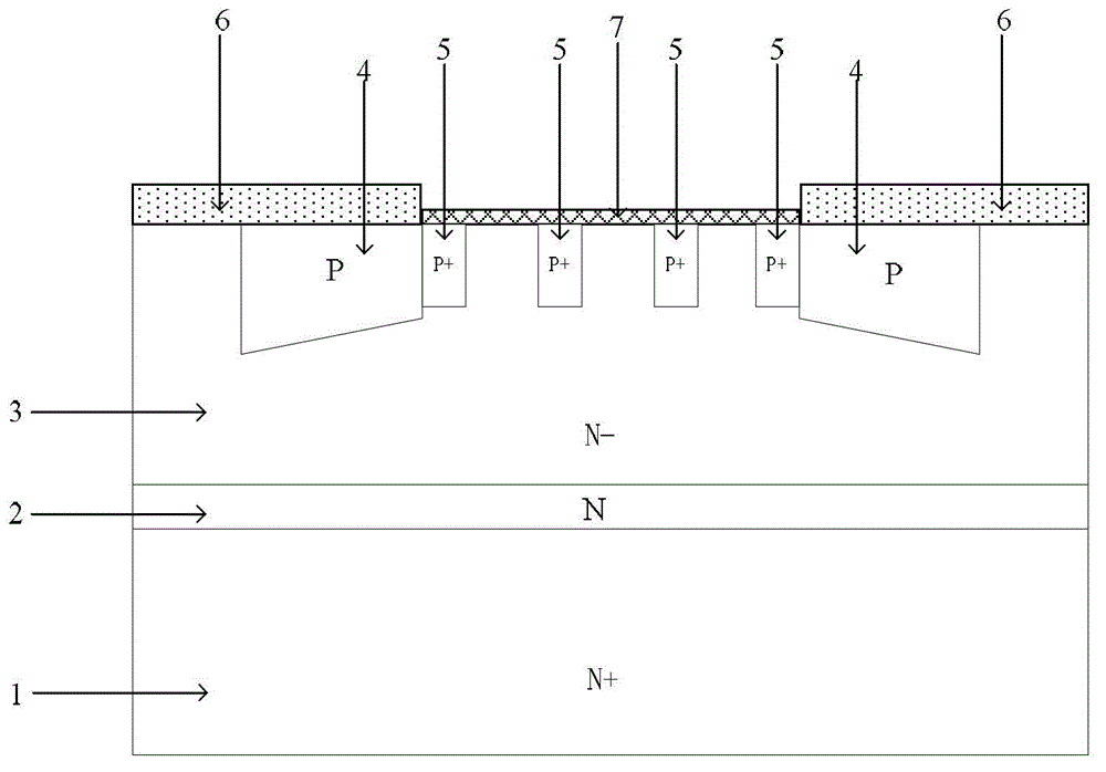
[0020] Attached below figure 2 , the present invention is described in detail, a silicon carbide junction barrier Schottky diode device with a ladder-shaped terminal, the silicon carbide junction barrier Schottky diode device with a ladder-shaped terminal is a symmetrical structure, including: an N+ type substrate 1, An N-type transition epitaxial layer 2 is provided on the N+ type substrate 1, an N-type epitaxial layer 3 is provided on the N-type transition epitaxial layer 2, and two P-type junctions are provided above the inside of the N-type epitaxial layer 3. Terminal 4 and 4 equally spaced P+ type body regions 5, and the inner edges of the two P type junction terminals 4 are offset against the outer edges of the adjacent two P+ type body regions 5, and the upper surface of the N-type epitaxial layer 3 is set There are two field oxide layers 6 and metal layers 7, the inner boundaries of the two P-type junction terminals 4 are respectively aligned with the inner boundaries...


PUM


Abstract

The invention discloses a silicon carbide junction barrier Schottky diode device with trapezoid terminals. The silicon carbide junction barrier Schottky diode device with trapezoid terminals are in a symmetrical structure and comprises an N+ type substrate, wherein an N type transitional epitaxial layer is arranged on the N+ type substrate, an N- type epitaxial layer is arranged on the N type transitional epitaxial layer, two P type node terminals and four P+ type body regions at equal intervals are arranged above the inner portion of the N- type epitaxial layer, inner edges of the two P type node terminals abuts against outer edges of two adjacent P+ type body regions, two field oxides and a metal layer are arranged on the outer surface of the N- type epitaxial layer, inner boundaries of the two P type node terminals are aligned to inner boundaries of the two field oxides respectively, two boundaries of the metal layer abut against inner boundaries of the two field oxides respectively, P type node terminals are in the trapezoid structure, and outer edges are longer than inner edges. By the aid of the structure, the electric field intensity distribution of a high field area can be optimized, so that the reverse characteristic of the device can be improved effectively, and the reliability of the device can be improved.

Description

technical field [0001] The invention mainly relates to the field of high-voltage power semiconductor devices, specifically, a silicon carbide junction barrier Schottky diode device with trapezoidal terminals, which is suitable for high-power rectification, inverter freewheeling, and power factor correction (PFC) systems . Background technique [0002] With the continuous improvement of people's living standards, electronic products continue to put forward new requirements for volume, performance, reliability and cost. However, many commercial power devices are approaching the theoretical limits limited by silicon materials, given their low ability to block high voltages. In this situation, silicon carbide technology came out. Silicon carbide has a series of properties superior to silicon, such as an order of magnitude higher breakdown electric field, three times the forbidden band width, and three times the thermal conductivity of silicon, which makes silicon carbide high-...

Claims


Application Information

Patent Timeline
Patent Type & Authority Patents(China)
IPC IPC(8): H01L29/872H01L29/06
CPCH01L29/872
Inventor 刘斯扬杨超张春伟钱钦松孙伟锋陆生礼时龙兴
Owner SOUTHEAST UNIV
Features
  • R&D
  • Intellectual Property
  • Life Sciences
  • Materials
  • Tech Scout
  • Unparalleled Data Quality
  • Higher Quality Content
  • 60% Fewer Hallucinations
Learn More