Storer

A memory and source storage technology, applied in the field of memory, can solve the problems of memory consumption of single-crystal silicon substrates, difficulty in manufacturing a combined substrate read-only memory, etc., and achieve the effects of easy manufacturing and saving of single-crystal silicon substrates

Active Publication Date: 2015-07-29
于翔
View PDF8 Cites 1 Cited by
  • Summary
  • Abstract
  • Description
  • Claims
  • Application Information

AI Technical Summary

Problems solved by technology

[0004] The purpose of the present invention is to overcome the disadvantages that the single-crystal silicon substrate of large area is consumed by the memory containing the passive memory unit circuit, and the combination substrate read-only memory is difficult to manufacture, and a kind of memory is provided.

Method used


Image

  • Storer
  • Storer
  • Storer

Examples


Embodiment

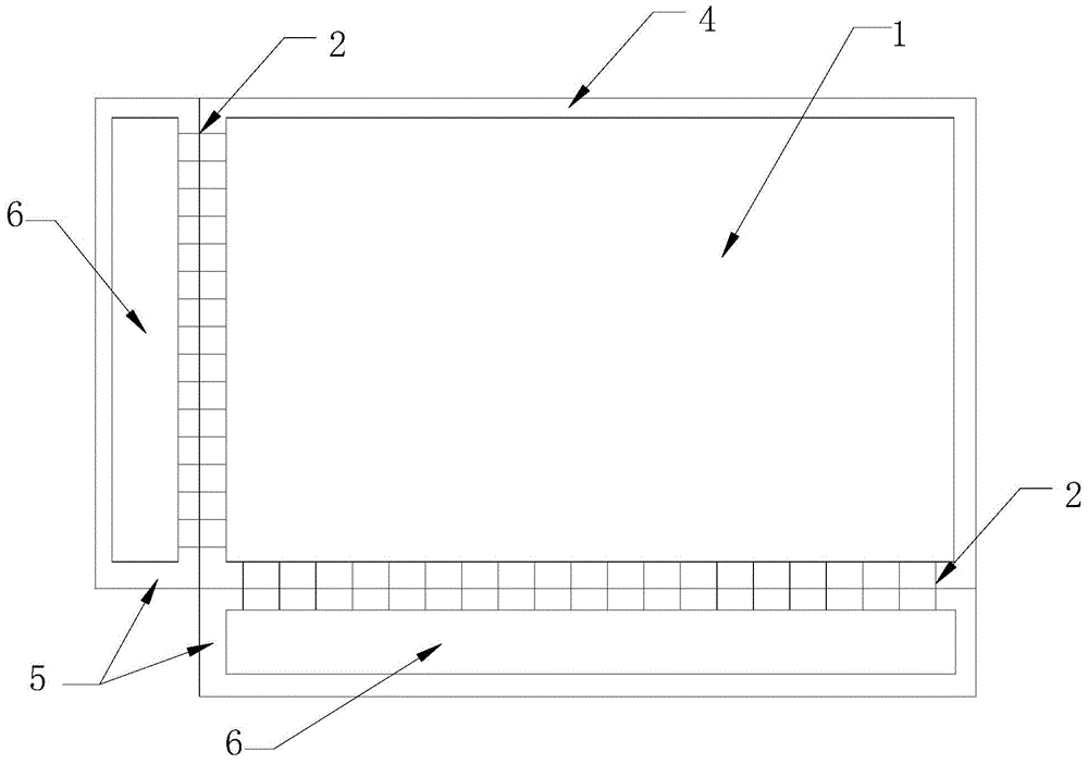
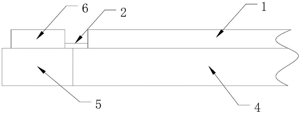
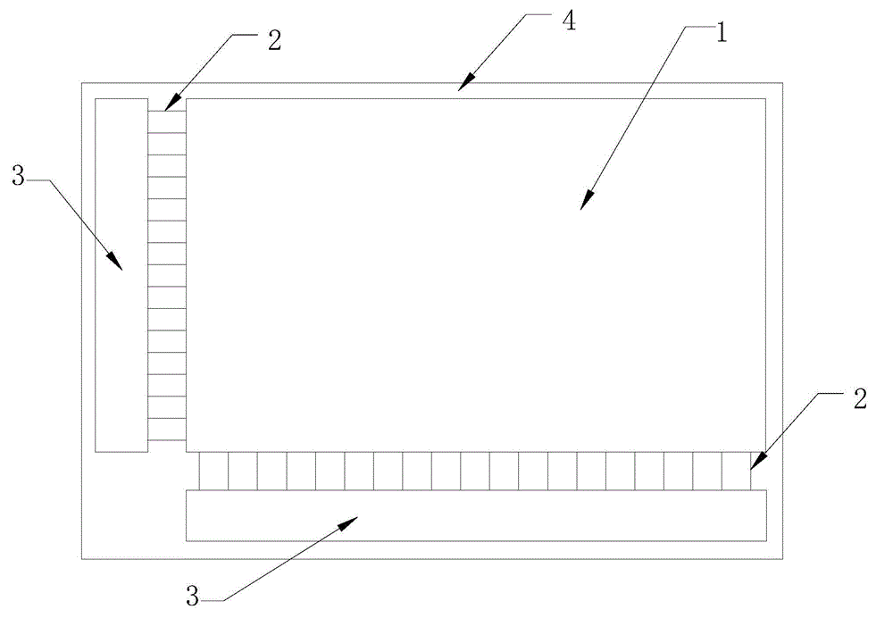
[0022] The structural diagram of the memory of the embodiment of the present invention is as follows image 3 , its cross-sectional diagram is shown in Figure 4 . The memory is composed of two control chips 3 , a passive memory cell matrix circuit 1 and a lead row 2 located on an insulating substrate 4 .

[0023] Same as the prior art, the passive memory cell matrix circuit 1 and the lead row 2 are located on the insulating substrate 4, and the passive memory cell matrix circuit 1 includes metal word lines, metal bit lines, and metal word lines and metal bit lines. The conductive material, the metal word line and the metal bit line are respectively connected to the lead row 2, the control chip 3 includes a monocrystalline silicon substrate 5 and a circuit unit 6, the circuit unit 6 is arranged on the monocrystalline silicon substrate 5, and the circuit unit 6 passes through the lead wire Bank 2 is connected to passive memory cell matrix circuit 1 . The circuit unit 6 here ...


PUM


Abstract

The invention relates to the technology of storers and solves problems that a large-area monocrystalline silicon substrate is consumed in a storer containing a passive storage unit circuit and the read-only storer of a combined substrate is hard to make. According to the technical scheme, the storer comprises an insulating substrate, a passive storage unit matrix circuit, a lead line and at least one control chip, the passive storage unit matrix circuit and the lead line are arranged on the upper surface of the insulating substrate, the control chips are in circuit connection with the passive storage unit matrix circuit through the lead line, and the control chips are reversely installed on the upper surface of the insulating substrate. The storer has the advantages of being easy to make and suitable to the real-only storer.

Description

technical field [0001] The present invention relates to memory technology. Background technique [0002] Common memories, such as random access memory, read-only memory and flash memory including active memory unit circuits, resistive memory including passive memory unit circuits, phase-change memory and other memories, are manufactured on a monocrystalline silicon substrate. Memory unit circuits, drive circuits, peripheral circuits, etc. are located on a single crystal silicon substrate. For example, a mask read-only memory disclosed in Chinese patent application number "92109280.6", and a multilayer cross-point resistance memory disclosed in Chinese patent application number "201010175802.8" and its manufacturing method are all circuits integrated in a single crystal On the substrate, although this is easier to manufacture, it will consume a larger area of ​​single crystal silicon substrate, and the cost is higher. [0003] And as Chinese patent application number is " 9...

Claims


Application Information

Patent Timeline
IPC IPC(8): H01L25/18
Inventor 于翔
Owner 于翔
Why Eureka
Try Eureka