Light-emitting diode epitaxial wafer, manufacturing method thereof, light-emitting diode chip manufacturing method, and substrate recycling method

A technology of light-emitting diodes and epitaxial wafers, applied in semiconductor/solid-state device manufacturing, electrical components, electrical solid-state devices, etc., to achieve the effects of reducing environmental pollution, reducing costs, and small lattice mismatch

Active Publication Date: 2015-07-29
HC SEMITEK SUZHOU
View PDF7 Cites 8 Cited by
  • Summary
  • Abstract
  • Description
  • Claims
  • Application Information

AI Technical Summary

Problems solved by technology

[0005] In order to solve the problem of reducing the production cost of LED epitaxial wafers and reducing environmental pollution, the embodiment of the present invention provides a light-emitting diode epitaxial wafer and its preparation method, light-emitting diode chip preparation and substrate recovery method

Method used


Image

  • Light-emitting diode epitaxial wafer, manufacturing method thereof, light-emitting diode chip manufacturing method, and substrate recycling method
  • Light-emitting diode epitaxial wafer, manufacturing method thereof, light-emitting diode chip manufacturing method, and substrate recycling method
  • Light-emitting diode epitaxial wafer, manufacturing method thereof, light-emitting diode chip manufacturing method, and substrate recycling method

Examples


Embodiment 1

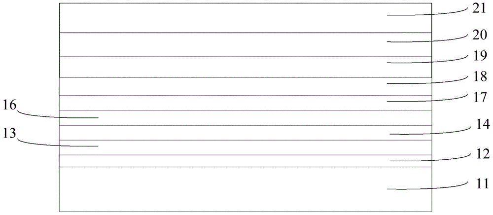
[0054] An embodiment of the present invention provides a light emitting diode epitaxial wafer, see figure 1 , the light emitting diode (Light Emiting Diode, LED for short) epitaxial wafer includes a GaAs substrate 11 and a first epitaxial layer grown on the GaAs substrate 11 .

[0055] Wherein, the first epitaxial layer includes an N-type GaAs buffer layer 12 on the GaAs substrate 11, a first N-type Ga X In 1-X P layer 13 , N-type GaAs layer 14 , N-type AlAs sacrificial layer 16 , N-type GaInP etch stop layer 17 , N-type GaAs ohmic contact layer 18 , N-type AlInP layer 19 , quantum well layer 20 , and P-type layer 21 . 0.47

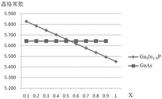
[0056] Among them, the first N-type Ga X In 1-X The lattice constants of the P layer, the N-type GaAs layer, and the N-type AlAs sacrificial layer are similar to those of the GaAs substrate and the AlGaInP LED epitaxial layer materials, and the lattice mismatch is small. figure 2 shows the Ga X In 1-X Lattice constants of P and GaAs. When...

Embodiment 2

[0063] The embodiment of the present invention provides a method for preparing an epitaxial wafer of a light emitting diode, which is suitable for preparing an epitaxial wafer of an AlGaInP LED. see Figure 5 , the method includes:

[0064] Step 201, providing a GaAs substrate.

[0065] Step 202, growing a first epitaxial layer on the GaAs substrate to obtain an LED epitaxial wafer.

[0066] Wherein, the first epitaxial layer includes an N-type GaAs buffer layer, a first N-type Ga X In 1-X P layer, N type GaAs layer, N type AlAs sacrificial layer, N type GaInP etch stop layer, N type GaAs ohmic contact layer, N type AlInP layer, quantum well layer, and P type layer. 0.47

[0067] Optionally, the first N-type Ga X In 1-X The growth conditions of the P layer include growth temperature of 640-660 degrees, TMGa flow of 40-50sccm, TMIn flow of 800-850sccm, PH3 flow of 900-1100sccm, thickness of 100-300nm, doping concentration of 1e-18~ 5e-18, the lattice mismatch is...

Embodiment 3

[0075] The embodiment of the present invention provides a method for preparing a light emitting diode chip, which is suitable for preparing an AlGaInP LED chip. see Figure 6 , the method includes:

[0076] Step 301, providing a first epitaxial wafer.

[0077] Wherein the structure of the first epitaxial wafer is the same as that of the LED epitaxial wafer provided in Embodiment 1, and will not be repeated here.

[0078] Step 302, bonding the first epitaxial wafer to the first substrate.

[0079] Among them, see Figure 7 , the first epitaxial layer 10 is located between the GaAs substrate 11 and the first substrate 30 .

[0080] The prepared first epitaxial wafer can be bonded to the first substrate through a metal bonding process, and the material of the first substrate can be Si, sapphire, flexible conductive polyester resin (English: Polyethylene Terephthalate, abbreviated: PET or PEIT), or copper.

[0081] Since the epitaxial layer is very thin, the first epitaxial ...


PUM


Abstract

The invention discloses a light-emitting diode epitaxial wafer, a manufacturing method thereof, a light-emitting diode chip manufacturing method, and a substrate recycling method, which belongs to the field of light-emitting diodes. The light-emitting diode epitaxial wafer comprises a GaAs substrate, and a first epitaxial layer growing on the GaAs substrate, wherein the first epitaxial layer comprises an N-type GaAs buffer layer, a first N-type GaXIn1-XP layer, an N-type GaAs layer, an N-type AlAs sacrificial layer, an N-type GaInP etching stop layer, an N-type GaAs ohmic contact layer, an N-type AlInP layer, a quantum well layer and a P-type layer located on the GaAs substrate in sequence, and X is larger than 0.47 but smaller than 0.51. The light-emitting diode epitaxial wafer manufacturing method comprises steps: the GaAs substrate is provided; the first epitaxial layer grows on the GaAs substrate; and the light-emitting diode epitaxial wafer is obtained. According to the embodiment of the invention, the GaAs substrate is stripped from the first epitaxial wafer, the GaAs substrate is not fully damaged, and environmental pollution is reduced; and the stripped GaAs substrate is used for manufacturing the epitaxial wafer again, repeated use of the GaAs substrate is realized, and the cost of the LED epitaxial wafer is greatly reduced.

Description

technical field [0001] The invention relates to the field of light-emitting diodes, in particular to a light-emitting diode epitaxial wafer and a preparation method thereof, a light-emitting diode chip preparation and a substrate recycling method. Background technique [0002] In recent years, AlGaInP light-emitting diodes (Light Emiting Diodes, LEDs for short) with high luminance characteristics have been widely used in more and more application fields, and the market demand is constantly expanding. [0003] AlGaInP LED epitaxial wafers include GaAs substrates and epitaxial layers grown on GaAs substrates. After completing the preparation of the AlGaInP LED epitaxial wafer, the chip process will be carried out. In the chip process stage, the substrate needs to be removed. The existing method for removing the substrate is to remove the substrate by grinding or the like. After grinding, the substrate will be completely destroyed. In this way, only one AlGaInP LED epitaxia...

Claims


Application Information

Patent Timeline
Patent Type & Authority Applications(China)
IPC IPC(8): H01L33/12H01L33/02H01L33/00H01L21/683
CPCH01L21/6835H01L33/0062H01L33/0093H01L33/02H01L33/12H01L2221/68381
Inventor 邢振远董耀尽王世俊李彤
Owner HC SEMITEK SUZHOU
Why Eureka
Try Eureka