MEMS inertial sensor and making method of same

An inertial sensor and manufacturing method technology, applied in instruments, measuring devices, etc., can solve the problems of small space for continuous improvement of chip performance, reduce chip size, etc., to meet the requirements of miniaturization development, improve utilization rate, and improve signal-to-noise ratio. Effect

Active Publication Date: 2015-08-05
GOERTEK MICROELECTRONICS CO LTD
View PDF5 Cites 3 Cited by
  • Summary
  • Abstract
  • Description
  • Claims
  • Application Information

AI Technical Summary

Problems solved by technology

The current problem is that the development of the MEMS process is relatively mature, and the process capability is close to the limit. It is difficult to further reduce the size of the chip according to the requirements of the system manufacturer, and there is little room for the chip performance to continue to improve.

Method used


Image

  • MEMS inertial sensor and making method of same
  • MEMS inertial sensor and making method of same
  • MEMS inertial sensor and making method of same

Examples


Embodiment Construction

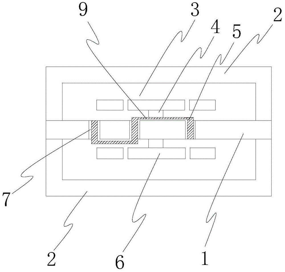
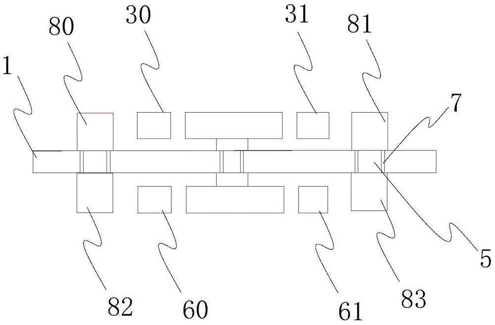
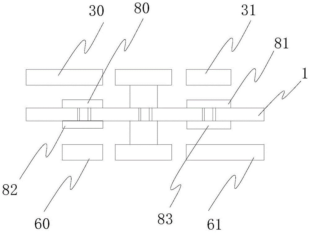
[0032] Various exemplary embodiments of the present invention will now be described in detail with reference to the accompanying drawings. It should be noted that the relative arrangements of components and steps, numerical expressions and numerical values ​​set forth in these embodiments do not limit the scope of the present invention unless specifically stated otherwise.

[0033] The following description of at least one exemplary embodiment is merely illustrative in nature and in no way taken as limiting the invention, its application or uses.

[0034] Techniques, methods and devices known to those of ordinary skill in the relevant art may not be discussed in detail, but where appropriate, such techniques, methods and devices should be considered part of the description.

[0035] In all examples shown and discussed herein, any specific values ​​should be construed as exemplary only, and not as limitations. Therefore, other instances of the exemplary embodiment may have dif...


PUM


Abstract

The invention discloses an MEMS inertial sensor and a making method of the same. The MEMS inertial sensor includes a substrate, and two cover bodies which are respectively fixed on an upper end and a lower end of the substrate. A first accommodating chamber and a second accommodating chamber are respectively formed by the two cover bodies and the substrate at the two sides of the substrate. At the upper end of the substrate, a first sensitive structure is arranged in the first accommodating chamber through a middle combining layer. At the lower end of the substrate, a second sensitive structure is arranged in the second accommodating chamber through a middle combining layer. According to the MEMS inertial sensor, the substrate is arranged at the middle of a chip and sensitive structures are bonded to the upper surface and the lower surface respectively of the substrate, so that the MEMS inertial sensor has a double-layer sensitive structure, thereby increasing the utilization ratio of chip area, improving the total performance of the MEMS inertial sensor, increasing the sensitivity by one times and increasing signal-noise ratio; in other words, the MEMS inertial sensor, compared with a conventional MEMS inertial sensor, on the basis of not reducing the performance of the chip, is further reduced in size, thereby satisfying small-size development of electronic products.

Description

technical field [0001] The present invention relates to an inertial measurement device, more specifically, to an inertial measurement device manufactured based on MEMS, such as a MEMS accelerometer, a gyroscope, an oscillator, etc.; the present invention also relates to a method for manufacturing a MEMS inertial sensor. Background technique [0002] At present, with the development of consumer electronics and wearable devices, higher and higher requirements are put forward for the performance of MEMS inertial sensors. Many system manufacturers hope that MEMS inertial devices can further reduce the chip size on the basis of maintaining the existing performance. In the current MEMS inertial device, the sensitive structure layer is anchored on the substrate by bonding, and the MEMS sealing cover is bonded on the upper surface of the sensitive structure layer to form a sealed cavity isolated from the outside world. The current problem is that the development of MEMS technology i...

Claims


Application Information

Patent Timeline
Patent Type & Authority Applications(China)
IPC IPC(8): G01C25/00
CPCG01C25/00
Inventor 郑国光
Owner GOERTEK MICROELECTRONICS CO LTD
Why Eureka
Try Eureka