Bandgap voltage reference source circuit

A reference voltage source and reference circuit technology, applied in the direction of adjusting electrical variables, control/regulation systems, instruments, etc., can solve the problems of increasing layout area, increasing reference voltage offset voltage, large area, etc., to improve product yield, The effect of reducing the occupied area and avoiding the influence of offset voltage

Inactive Publication Date: 2015-08-05
SHENZHEN XINLIAN ELECTRONICS TECH CO LTD +1
View PDF4 Cites 3 Cited by
  • Summary
  • Abstract
  • Description
  • Claims
  • Application Information

AI Technical Summary

Problems solved by technology

[0007] The bandgap reference voltage circuit with the above structure has the problem of large area because it includes the error amplifier and the corresponding bias circuit, and the offset voltage and noise of the error amplifier itself will also be added to the refe

Method used


Image

  • Bandgap voltage reference source circuit
  • Bandgap voltage reference source circuit
  • Bandgap voltage reference source circuit

Examples


Embodiment Construction

[0021] In order to make the object, technical solution and advantages of the present invention clearer, the present invention will be further described in detail below in conjunction with the accompanying drawings and embodiments. It should be understood that the specific embodiments described here are only used to explain the present invention, not to limit the present invention.

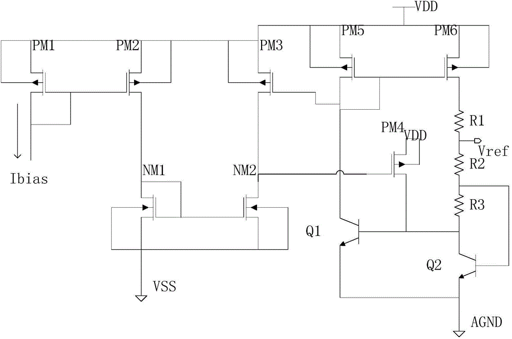
[0022] An embodiment of the present invention provides a bandgap reference voltage source circuit, including: a reference circuit and a start-up circuit, such as figure 2 As shown, the reference circuit includes: a fifth PMOS transistor PM5, a sixth PMOS transistor PM6, a first NPN transistor, a second NPN transistor, a first resistor R1, a second resistor R2, a third resistor R3 and are used to generate and Power supply and temperature independent reference voltage output Vref.

[0023] The start-up circuit is used to provide the start-up bias voltage for the reference core circuit in a degenera...


PUM


Abstract

The invention relates to a bandgap voltage reference source circuit which comprises a reference circuit and a starting circuit, wherein the reference circuit comprises a fifth PMOS transistor, a six PMOS transistor, first NPN transistors, a second NPN transistor, a first resistor, a second resistor, and a third resistor, and is used for generating a voltage reference output Vref, the starting circuit provides starting offset voltage for a reference core circuit under degeneracy state and comprises a first PMOS transistor, a second PMOS transistor, a third PMOS transistor, a fourth PMOS transistor, a first NMOS transistor and a second NMOS transistor. The circuit is simply structured, and practical and is accurate in output.

Description

technical field [0001] The invention relates to a CMOS bandgap reference voltage source circuit, in particular to a CMOS bandgap reference voltage source circuit without an operational amplifier, and belongs to the technical field of analog integrated circuits. Background technique [0002] The basic principle of a bandgap voltage reference is to use two voltages with opposite temperature coefficients to add with appropriate weights to produce a voltage with zero temperature coefficient. A bipolar junction transistor (BJT) has the following two properties: the base-emitter voltage VBE of a bipolar transistor is inversely proportional to the absolute temperature; at different collector currents, the base-emitter voltage of two bipolar transistors Pole voltage difference ΔVBE is proportional to the absolute temperature. Therefore bipolar transistors are usually at the heart of forming a bandgap reference voltage. [0003] In the field of analog integrated circuit or mixed-si...

Claims


Application Information

Patent Timeline
IPC IPC(8): G05F1/565
Inventor 李彬欧健
Owner SHENZHEN XINLIAN ELECTRONICS TECH CO LTD
Why Eureka
Try Eureka