Manufacturing method of inversion structure of III semiconductor light-emitting device

A technology for light-emitting devices and manufacturing methods, which is applied to semiconductor devices, electrical components, circuits, etc., can solve the problems of high etching holes, complicated processes, and high production costs, achieve simplified manufacturing processes, omit metal protective layers, and solve the problem of transparent conductive layers and Effect of line convex mesa pattern alignment

Active Publication Date: 2015-08-05
XIANGNENG HUALEI OPTOELECTRONICS
View PDF4 Cites 25 Cited by
  • Summary
  • Abstract
  • Description
  • Claims
  • Application Information

AI Technical Summary

Problems solved by technology

[0002] Traditional light-emitting diodes adopt a front-mount structure. Generally, the transparent conductive layer is made of high-transmittance materials, such as ITO, AZO, etc., and the electrodes are generally made of Cr/Pt/Au, etc. However, in the flip-chip structure, the light excited by the active layer It is directly emitted from the substrate on the other side of the electrode, so the requirement for the P-type electrode is changed to a highly reflective material covering the entire p-type nitride semiconductor layer as a mirror structure. The first is on the p-type nitride semiconductor layer Plating a transparent electrode with high transmittance plus high reflective metal, such as ITO/Ag, etc., the other is to directly coat a high reflective metal on the p-type nitride semiconductor layer as an ohmic contact layer and a mirror, For example, Ag, Al, etc., no matter wh

Method used


Image

  • Manufacturing method of inversion structure of III semiconductor light-emitting device
  • Manufacturing method of inversion structure of III semiconductor light-emitting device
  • Manufacturing method of inversion structure of III semiconductor light-emitting device

Examples


Embodiment 1

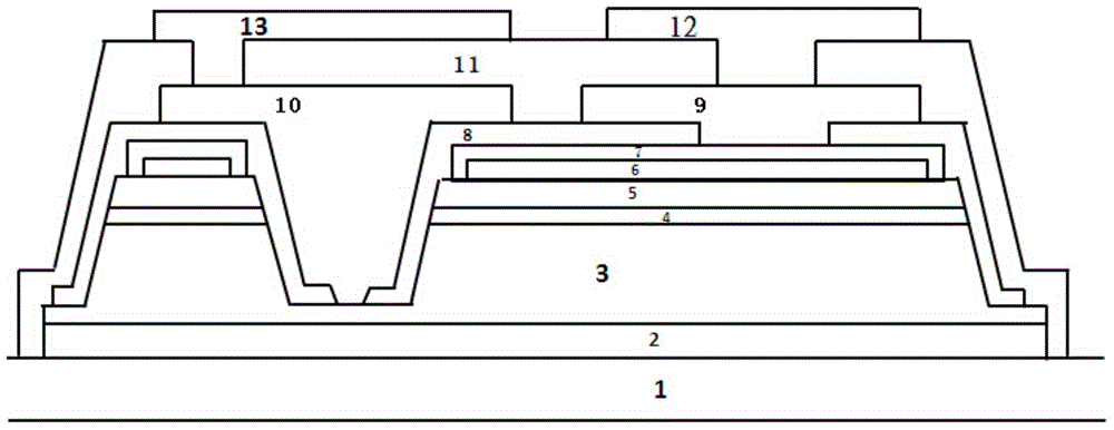
[0046] This embodiment provides a method for fabricating a flip-chip structure of a Group III semiconductor light-emitting device. For details, see Figure 2a-Figure 2g , including the following steps:

[0047] The first step: the structure diagram is as follows Figure 2a As shown, the method is to sequentially grow the substrate 1, the buffer layer 2, the n-type nitride semiconductor layer 3, the active layer 4, and the p-type nitride semiconductor layer 5 to form an epitaxial structure, and the epitaxial structure The upper surface of the upper surface is the upper surface of the p-type nitride semiconductor layer 5, and this structure is an epitaxial structure, which is obtained through the manufacturing process in the prior art. The method for making a flip chip on the epitaxial structure includes the following steps:

[0048] The second step: the structure diagram is as follows Figure 2b As shown, the method is to deposit a transparent conductive layer 14 on the upper...

Embodiment 2

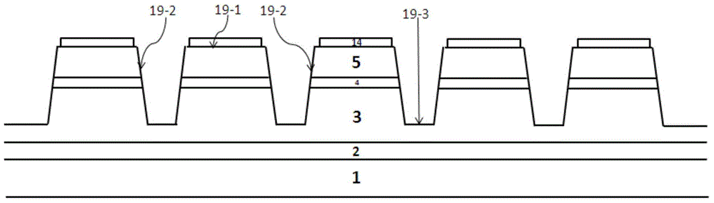
[0085] The new structure of the present invention adopts the technology of linear convex mesa 19 to replace the technology of multiple vias.

[0086] Such as Figure 3a Shown is a top view of a plurality of vias in the prior art, Figure 3b for Figure 3a Sectional view along the A-B direction.

[0087] Such as Figure 4a Shown is a top view of a linear convex table top, Figure 4b for Figure 4a Sectional view along the A-B direction.

[0088] The etched area of ​​the line convex mesa 19 is single or multiple lines;

[0089] The substrate 1, the buffer layer 2, the n-type nitride semiconductor layer 3, the active layer 4 and the p-type nitride semiconductor layer 5 form a nitride semiconductor structure with a line convex mesa 19;

[0090] The linear convex mesa includes a first upper surface 19-1, a side surface 19-2 and a second upper surface 19-3, and the two ends of the first upper surface are respectively provided with the side surface and the second upper surface...

Embodiment 3

[0093] The lower end of the P-type wire electrode 15 is arranged on the surface of the first insulating layer structure 8-1 and on the transparent conductive layer 14 (such as Figure 5 shown).


PUM

PropertyMeasurementUnit
Thicknessaaaaaaaaaa
Thicknessaaaaaaaaaa
Thicknessaaaaaaaaaa

Abstract

The application discloses a manufacturing method of an inversion structure of a III semiconductor light-emitting device. The manufacturing method comprises the following steps: growing a substrate, a buffer layer, an n type nitride semiconductor layer, an active layer, and a p type nitride semiconductor layer successively from bottom to top to form an epitaxial structure; depositing a transparent conductive layer; carrying out yellow-light etching process and definition to form an isolation slot; depositing a first insulation layer structure; depositing a P type contact metal unit and an N type contact metal unit simultaneously; depositing a second insulation layer structure; depositing an inverted P type electrode and an inverted N type electrode and removing a photoresistor by using a stripping process so as to obtain a wafer; and carrying out reduction, scribing, splitting, testing ,and sorting on the wafer. According to the invention, the linear convex table surface technology is used for replacing the multi-hole vias technology in the prior art. The first insulation layer structure is a Bragg reflection layer-metal level-multilayer oxide insulating layer unit and serves as a reflector structure and an insulation layer, and thus an inverted reflector structure design and a first insulation layer are replaced and a metal protection layer is also removed.

Description

technical field [0001] The present application relates to the technical field of semiconductor lighting, in particular, to a method for fabricating a flip-chip structure of a Group III semiconductor light-emitting device. Background technique [0002] Traditional light-emitting diodes adopt a front-mount structure. Generally, the transparent conductive layer is made of high-transmittance materials, such as ITO, AZO, etc., and the electrodes are generally made of Cr / Pt / Au, etc. However, in the flip-chip structure, the light excited by the active layer It is directly emitted from the substrate on the other side of the electrode, so the requirement for the P-type electrode is changed to a highly reflective material covering the entire p-type nitride semiconductor layer as a mirror structure. The first is on the p-type nitride semiconductor layer Plating a transparent electrode with high transmittance plus high reflective metal, such as ITO / Ag, etc., the other is to directly coa...

Claims


Application Information

Patent Timeline
IPC IPC(8): H01L33/00H01L33/38H01L33/46H01L33/42
CPCH01L33/0075H01L33/38H01L33/42H01L33/46H01L2933/0016H01L2933/0025
Inventor 许顺成蔡炳傑梁智勇
Owner XIANGNENG HUALEI OPTOELECTRONICS
Why Eureka
Try Eureka