Light-emitting diode epitaxial wafer and manufacturing method thereof

A technology of light-emitting diodes and manufacturing methods, which is applied in the direction of electrical components, circuits, semiconductor devices, etc., and can solve the problems that the luminous efficiency needs to be improved, and achieve the effect of improving efficiency and expanding current

Active Publication Date: 2015-08-05
HC SEMITEK SUZHOU
View PDF4 Cites 7 Cited by
  • Summary
  • Abstract
  • Description
  • Claims
  • Application Information

AI Technical Summary

Problems solved by technology

[0003] Existing epitaxial wafers include a sapphire substrate, a buffer layer, an undoped GaN layer, an N-type GaN layer, a multiple quantum well layer, a P-type electron blocking layer, and a P-type GaN layer stacked on the sapphire substrate in sequence. Luminous efficiency still needs to be improved

Method used


Image

  • Light-emitting diode epitaxial wafer and manufacturing method thereof
  • Light-emitting diode epitaxial wafer and manufacturing method thereof

Examples


Embodiment 1

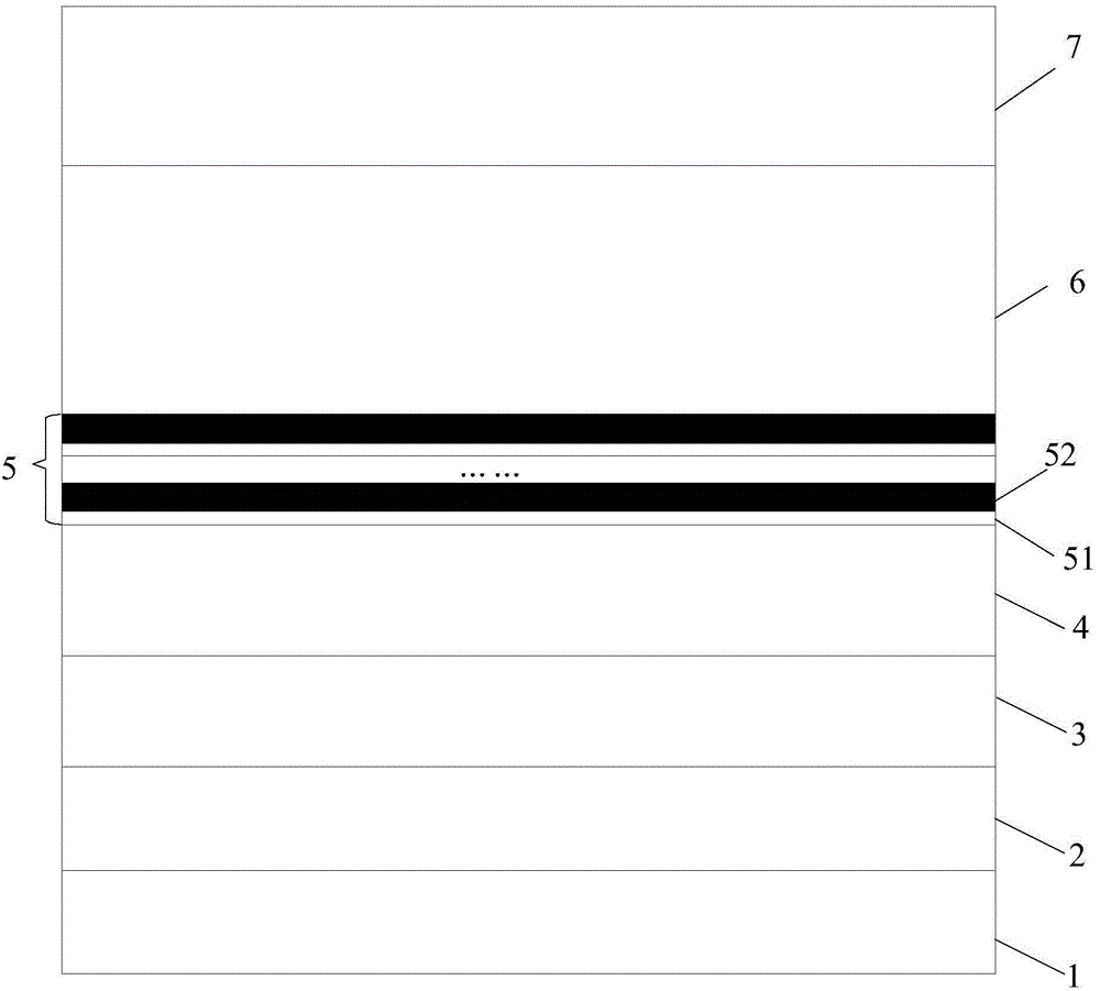
[0024] An embodiment of the present invention provides a light emitting diode epitaxial wafer, see figure 1 , the light-emitting diode epitaxial wafer includes a sapphire substrate 1, and a buffer layer 2, an undoped GaN layer 3, an N-type GaN layer 4, a current spreading layer 5, and a multi-quantum well layer 6 stacked sequentially on the sapphire substrate 1 and a p-type GaN layer 7 .

[0025] In this embodiment, the current spreading layer 5 includes alternately grown first sublayers 51 and second sublayers 52, the first sublayer 51 is formed of varistor material, and the second sublayer 52 is formed of N-type doped GaN , and the doping concentration of the second sub-layer 52 is lower than the doping concentration of the N-type GaN layer. It can be understood that if the doping concentration of the second sub-layer 52 is lower than that of the N-type GaN layer, it is beneficial for electrons to be injected into the MQW layer 6 from the N-type GaN layer 4 through the curr...

Embodiment 2

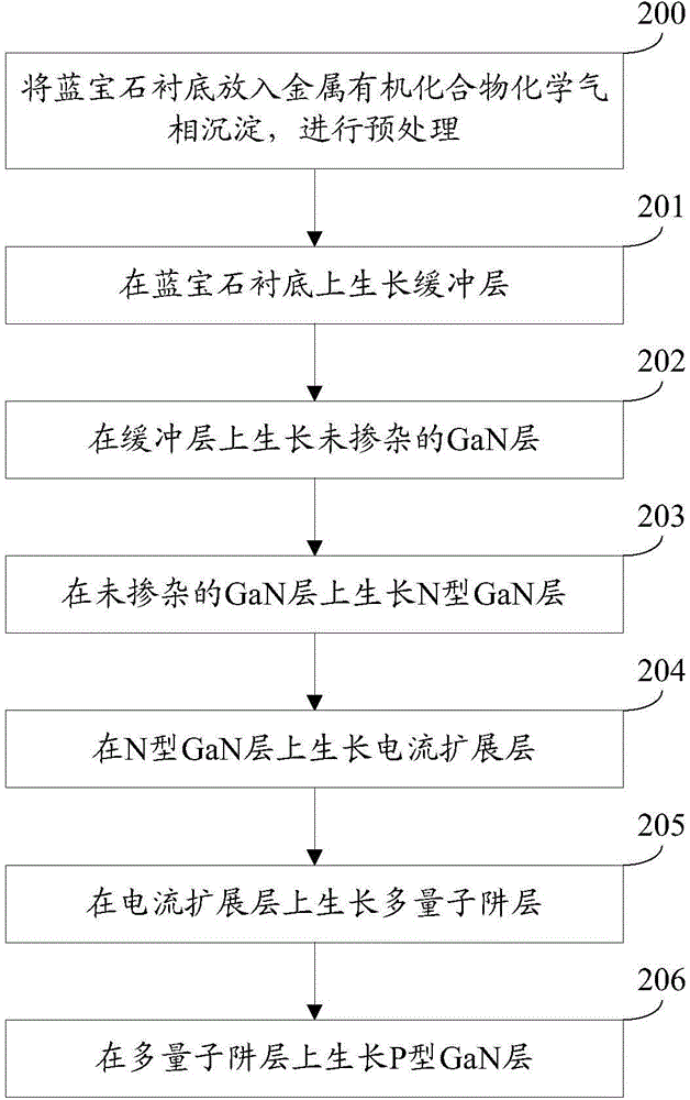
[0036] An embodiment of the present invention provides a method for manufacturing a light-emitting diode epitaxial wafer, see figure 2 , the manufacturing method includes:

[0037] Step 200: put the sapphire substrate into Metal Organic Chemical Vapor Deposition (MOCVD for short) for pretreatment.

[0038] Specifically, the sapphire substrate can be (0001) crystalline sapphire Al 2 o 3 .

[0039] Specifically, this step 200 may include:

[0040] Place the sapphire substrate in a hydrogen atmosphere for 10-15 minutes of high-temperature heat treatment at a temperature of 1000-1200 ° C to clean the surface of the substrate;

[0041] Nitriding treatment is performed on the sapphire substrate.

[0042] Step 201: growing a buffer layer on a sapphire substrate.

[0043] Specifically, the buffer layer may be a GaN layer.

[0044] Specifically, this step 201 may include:

[0045] Lower the temperature to 400-600°C, grow a GaN layer with a thickness of 15-35nm, and grow at a p...


PUM


Abstract

The invention discloses a light-emitting diode epitaxial wafer and a manufacturing method thereof and belongs to the semiconductor optoelectronic technical field. The light-emitting diode epitaxial wafer includes a sapphire substrate as well as a buffer layer, an undoped GaN layer, an N type GaN layer, a current spreading layer, a multi-quantum well layer and a P type GaN layer which are stacked on the sapphire substrate sequentially; the current spreading layer includes a first sub layer and a second sub layer which are grown alternately; the first sub layer is made of a variable resistance material; the second sub layer is made of N type doped GaN; and the doping concentration of the second sub layer is smaller than that of the N type GaN layer. According to the light-emitting diode epitaxial wafer and the manufacturing method thereof of the invention, the current spreading layer includes the first sub layer and the second sub layer which are grown alternately; the difference of lattice constants of the first sub layer and the second sub layer enables a polarization effect; charge distribution in the current spreading layer is nonuniform, so that an electric field can be formed, and current can be spread under the action of the electric field; and recombined luminescent electrons injected into the multi-quantum well layer are increased, and therefore, the efficiency of recombination luminescence can be improved.

Description

technical field [0001] The invention relates to the field of semiconductor optoelectronic technology, in particular to a light-emitting diode epitaxial wafer and a manufacturing method thereof. Background technique [0002] A light emitting diode (Light Emitting Diode, LED for short) is a semiconductor electronic component that can emit light, and epitaxial wafers are an important part of manufacturing light emitting diodes. [0003] Existing epitaxial wafers include a sapphire substrate, a buffer layer, an undoped GaN layer, an N-type GaN layer, a multiple quantum well layer, a P-type electron blocking layer, and a P-type GaN layer stacked on the sapphire substrate in sequence. The luminous efficiency still needs to be improved. Contents of the invention [0004] In order to solve the problems in the prior art, an embodiment of the present invention provides a light emitting diode epitaxial wafer and a manufacturing method thereof. Described technical scheme is as follo...

Claims


Application Information

Patent Timeline
Patent Type & Authority Applications(China)
IPC IPC(8): H01L33/06H01L33/32H01L33/00
CPCH01L33/0066H01L33/0075H01L33/06H01L33/14H01L33/32
Inventor 郭炳磊葛永晖吕蒙普谢文明陈柏松胡加辉魏世祯
Owner HC SEMITEK SUZHOU
Why Eureka
Try Eureka