

A kind of epitaxial wafer of light-emitting diode and its manufacturing method
A technology of light-emitting diodes and manufacturing methods, applied in semiconductor devices, electrical components, circuits, etc., can solve the problems of low electron recombination luminous efficiency, and achieve the effects of improving internal quantum efficiency, improving efficiency, and increasing the number of holes
- Summary
- Abstract
- Description
- Claims
- Application Information
AI Technical Summary
Problems solved by technology
Method used
Image

Examples
Embodiment 1
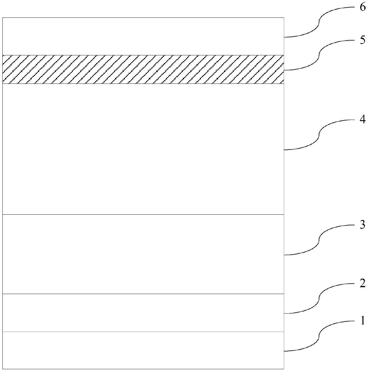
[0029] The embodiment of the present invention provides an epitaxial wafer of a light emitting diode, see figure 1 The epitaxial wafer includes a substrate 1 and a buffer layer 2, an undoped gallium nitride layer 3, an N-type gallium nitride layer 4, a light-emitting layer 5, and a P-type gallium nitride layer 6 sequentially stacked on the substrate 1.
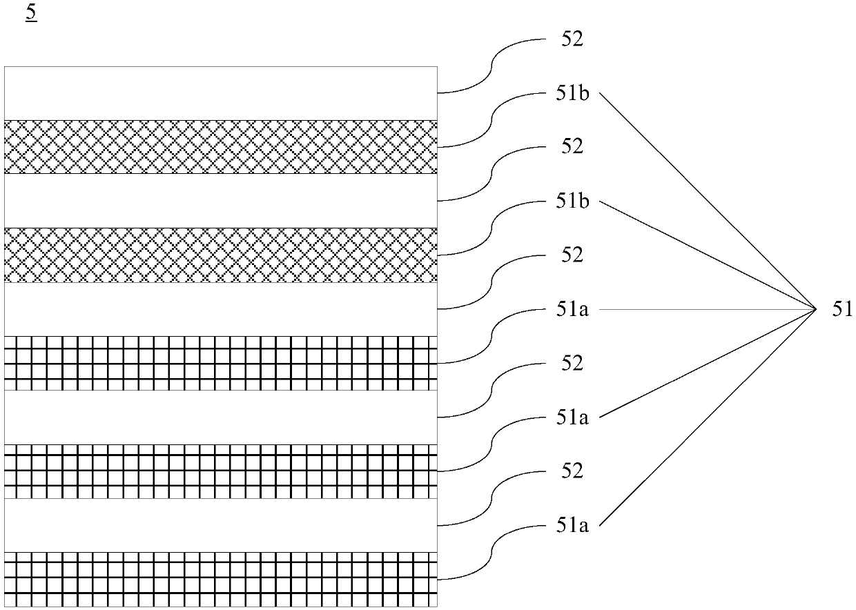
[0030] In this embodiment, see figure 2 The light emitting layer 5 includes a plurality of quantum well layers 51 and a plurality of quantum barrier layers 52. The plurality of quantum well layers 51 and the plurality of quantum barrier layers 52 are alternately stacked and arranged, and the quantum barrier layer 52 is a gallium nitride layer. At least three quantum well layers 51 of the plurality of quantum well layers 51 that are closest to the N-type gallium nitride layer 4 are the first quantum well layers 51a, and the plurality of quantum well layers 51 except for the first quantum well layer 51a The quantum well layer 51 is...
Embodiment 2
[0054] The embodiment of the present invention provides an epitaxial wafer for a light emitting diode, and the epitaxial wafer provided in this embodiment is a specific implementation of the epitaxial wafer provided in the first embodiment.
[0055] In this embodiment, the number of layers of the first quantum well layer is 3, and the number of layers of the second quantum well layer is 6, and the doping concentration of the P-type dopant in each second quantum well layer remains unchanged, and The doping concentrations of the P-type dopants in the plurality of second quantum well layers are equal.
Embodiment 3
[0057] The embodiment of the present invention provides an epitaxial wafer for a light emitting diode, and the epitaxial wafer provided in this embodiment is another specific implementation of the epitaxial wafer provided in the first embodiment.
[0058] In this embodiment, the number of layers of the first quantum well layer is 3, and the number of layers of the second quantum well layer is 6, and each second quantum well layer includes a first sublayer, a second sublayer, and a first sublayer that are sequentially stacked. Three sublayers, the second sublayer is a P-type doped indium gallium nitride layer, the first and third sublayers are undoped indium gallium nitride layers, the thickness of the first sublayer and the thickness of the third sublayer The thickness is equal, the thickness of the second sub-layer is 1 nm, and the doping concentration of the P-type dopant in the plurality of second quantum well layers is equal.
PUM
| Property | Measurement | Unit |
|---|---|---|
| thickness | aaaaa | aaaaa |
| thickness | aaaaa | aaaaa |
| temperature | aaaaa | aaaaa |
Abstract
Description
Claims
Application Information