A gallium nitride-based light-emitting diode epitaxial wafer and its growth method

A light-emitting diode, gallium nitride-based technology, applied in semiconductor devices, electrical components, circuits, etc., can solve the problem of electron overflow reducing composite luminous efficiency, etc., to improve composite luminous efficiency, slow down speed, and reduce non-radiative composite centers. Effect

Active Publication Date: 2021-08-03
HC SEMITEK SUZHOU
View PDF5 Cites 0 Cited by
  • Summary
  • Abstract
  • Description
  • Claims
  • Application Information

AI Technical Summary

Problems solved by technology

[0006] The embodiment of the present invention provides a gallium nitride-based light-emitting diode epitaxial wafer and its growth method, which can solve the problem of electron overflow reducing composite luminous efficiency in the prior art

Method used


Image

  • A gallium nitride-based light-emitting diode epitaxial wafer and its growth method
  • A gallium nitride-based light-emitting diode epitaxial wafer and its growth method

Examples


Embodiment Construction

[0025] In order to make the object, technical solution and advantages of the present invention clearer, the implementation manner of the present invention will be further described in detail below in conjunction with the accompanying drawings.

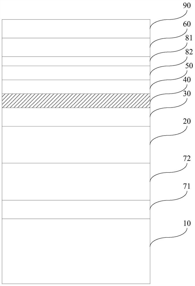
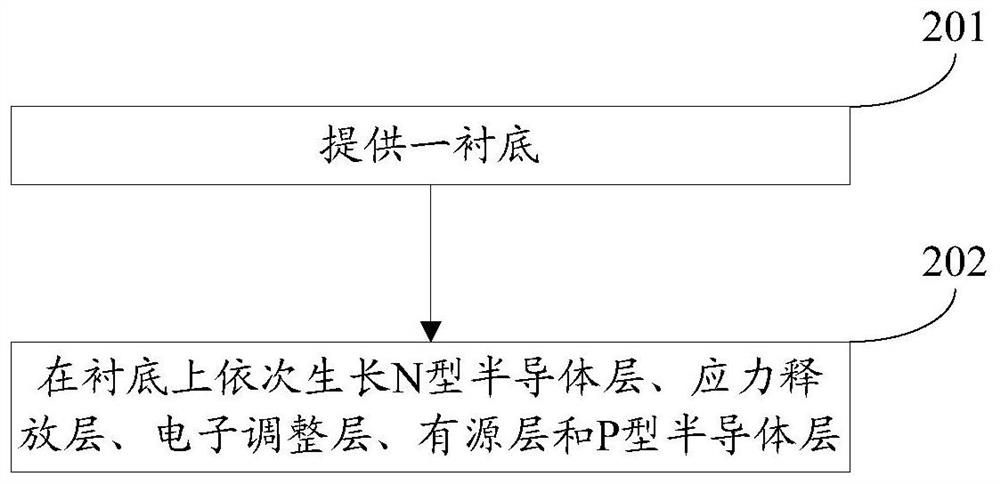
[0026] An embodiment of the present invention provides a GaN-based light-emitting diode epitaxial wafer. figure 1 A schematic structural diagram of a gallium nitride-based light-emitting diode epitaxial wafer provided by an embodiment of the present invention. see figure 1 , the GaN-based light-emitting diode epitaxial wafer includes a substrate 10, an N-type semiconductor layer 20, a stress release layer 30, an electronic adjustment layer 40, an active layer 50, and a P-type semiconductor layer 60, the N-type semiconductor layer 20, the stress release layer The layer 30 , the electron adjustment layer 40 , the active layer 50 and the P-type semiconductor layer 60 are sequentially stacked on the substrate 10 .

[0027] In this embodi...


PUM

PropertyMeasurementUnit
thicknessaaaaaaaaaa
thicknessaaaaaaaaaa
thicknessaaaaaaaaaa

Abstract

The invention discloses a gallium nitride-based light-emitting diode epitaxial wafer and a growth method thereof, belonging to the technical field of semiconductors. The gallium nitride-based light-emitting diode epitaxial wafer includes a substrate, an N-type semiconductor layer, a stress release layer, an active layer, and a P-type semiconductor layer, and the N-type semiconductor layer, the stress release layer, and the active layer and the P-type semiconductor layer are sequentially stacked on the substrate, and the gallium nitride-based light-emitting diode epitaxial wafer further includes an electronic adjustment layer, and the electronic adjustment layer is arranged on the stress release layer and the active layer Between; the material of the electronic adjustment layer is N-type doped aluminum gallium nitride, and the doping concentration of the N-type dopant in the electronic adjustment layer is along the stacking direction of the gallium nitride-based light-emitting diode epitaxial wafer slowing shrieking. The invention can improve the recombination luminous efficiency of electrons and holes in the active layer.

Description

technical field [0001] The invention relates to the technical field of semiconductors, in particular to a gallium nitride-based light-emitting diode epitaxial wafer and a growth method thereof. Background technique [0002] Light Emitting Diode (English: Light Emitting Diode, referred to as: LED) is a semiconductor diode that can convert electrical energy into light energy. Group III-V semiconductor materials are known as the third-generation semiconductor materials, which have excellent photoelectric properties. LEDs made of gallium nitride (GaN)-based materials among III-V semiconductor materials can emit various colors of light by controlling the composition of materials, which is the focus of research in the industry. [0003] Epitaxial wafers are the primary products in the LED manufacturing process. The existing LED epitaxial wafer includes a substrate, an N-type semiconductor layer, an active layer and a P-type semiconductor layer, and the N-type semiconductor layer...

Claims


Application Information

Patent Timeline
Patent Type & Authority Patents(China)
IPC IPC(8): H01L33/14H01L33/32H01L33/00
Inventor 王曼张琰琰陆香花周飚胡加辉
Owner HC SEMITEK SUZHOU
Why Eureka
Try Eureka