
Clock domain crossing AHB (advanced high-performance bus) bridging method and device

A technology across clock domains and clock domains, applied in the field of AHB bus bridging methods and devices, can solve the problems of increasing circuit area cost and logic design complexity, shortening R&D and design time, preventing pulse loss, area and design difficulty Reduced effect

Active Publication Date: 2015-08-19
DATANG MICROELECTRONICS TECH CO LTD +1
View PDF3 Cites 13 Cited by
  • Summary
  • Abstract
  • Description
  • Claims
  • Application Information

AI Technical Summary

Problems solved by technology

However, adding FIFO to prevent asynchronous data loss will increase the area cost and logic design complexity of the circuit

Method used


Image

  • Clock domain crossing AHB (advanced high-performance bus) bridging method and device
  • Clock domain crossing AHB (advanced high-performance bus) bridging method and device
  • Clock domain crossing AHB (advanced high-performance bus) bridging method and device

Examples


Embodiment Construction

[0019] In order to make the purpose, technical solution and advantages of the present invention more clear, the embodiments of the present invention will be described in detail below in conjunction with the accompanying drawings. It should be noted that, in the case of no conflict, the embodiments in the present application and the features in the embodiments can be combined arbitrarily with each other.

[0020] The steps shown in the flowcharts of the figures may be performed in a computer system, such as a set of computer-executable instructions. Also, although a logical order is shown in the flowcharts, in some cases the steps shown or described may be performed in an order different from that shown or described herein.

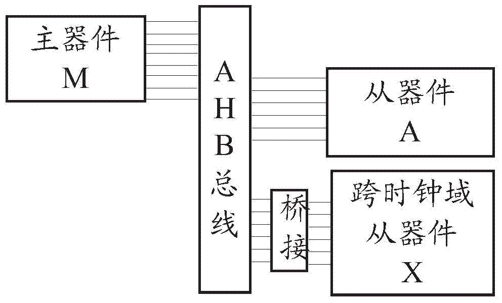
[0021] figure 1 It is a schematic diagram of an application scenario of AHB bus bridging across clock domains in an embodiment of the present invention. like figure 1 As shown, in a specific embodiment of the present invention, the master device M, the ...


PUM


Abstract

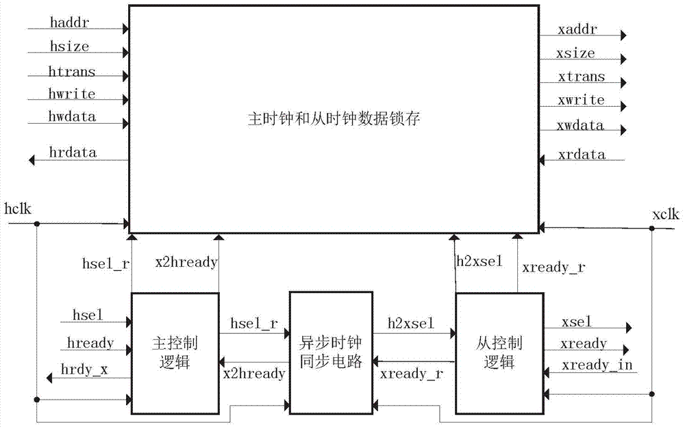
The invention discloses a clock domain crossing AHB (advanced high-performance bus) bridging method and device. The device comprises a master control logic module, a slave control logic module, a master clock and slave clock data latching module and an asynchronous pulse and synchronous circuit module. The master control logic module generates a bus control signal of a master clock domain according to a bus signal of a master device; the master control logic module generates a response signal fed back to the master device according to a slave device bus signal sampled in the master clock domain and latched by a slave clock domain; the slave control logic module generates a bus control signal of the slave clock domain according to a response signal of a slave device and a master device bus signal sampled in the slave clock domain and latched by the master clock domain; when the bus control signal is effectively enabled, the master clock and slave clock data latching module latches and samples synchronous data; the asynchronous pulse and synchronous circuit module synchronizes clock domain crossing signals to an opposite-party clock domain. The clock domain crossing AHB bridging method and device have the advantage that the master and slave devices can implement the AHB protocol under any frequency.

Description

technical field [0001] The invention relates to the technical field of AHB (Advanced High performance Bus, advanced high performance bus), in particular to a cross-clock domain AHB bus bridging method and device. Background technique [0002] With the increase of SOC (System on Chip, System on Chip) integrated circuit function complexity and the promotion of IP (Internet Protocol, Internet Protocol) multiplexing design, on-chip bus design has become a key issue. The AMBA (Advanced Microcontroller Bus Architecture, Advanced Microcontroller Bus Architecture) AHB bus introduced by ARM is widely used in data transmission. In the early chip design based on the AHB bus, both the master device and the slave device work in the same clock domain. In modern low-power design, multi-clock domain management is an effective way to reduce power consumption, so that different devices work on different clocks, such as low-frequency clock modules in a low-power state. However, when working ...

Claims


Application Information

Patent Timeline
IPC IPC(8): G06F13/40G06F13/42
CPCG06F13/405G06F13/4295
Inventor 刘小雷郝晓东
Owner DATANG MICROELECTRONICS TECH CO LTD
Learn More