Capacitive fingerprint sensor and fingerprint imaging module

A fingerprint sensor and capacitive technology, applied in the direction of acquiring/organizing fingerprints/palmprints, instruments, printing image collection, etc., can solve the problems of occupied area, high cost, and increase, so as to reduce device manufacturing cost and process complexity , The effect of reducing the difficulty of the process

Active Publication Date: 2015-08-26
SHANGHAI OXI TECH
View PDF3 Cites 23 Cited by
  • Summary
  • Abstract
  • Description
  • Claims
  • Application Information

AI Technical Summary

Problems solved by technology

In this capacitive fingerprint sensor, the sensing plate 33 and the receiving circuit 35 are all arranged on the same surface of the chip 30. Although the formation of through holes can be avoided and the cost can be reduced, the receiving circuit 35 occupies the area of ​​the sensing plate 33. , which is not conducive to the improvement of the accuracy of fingerprint image acquisition
[0010] However, the fingerprint sensor technology in the prior art is complicated and the cost is high

Method used


Image

  • Capacitive fingerprint sensor and fingerprint imaging module
  • Capacitive fingerprint sensor and fingerprint imaging module
  • Capacitive fingerprint sensor and fingerprint imaging module

Examples


Embodiment Construction

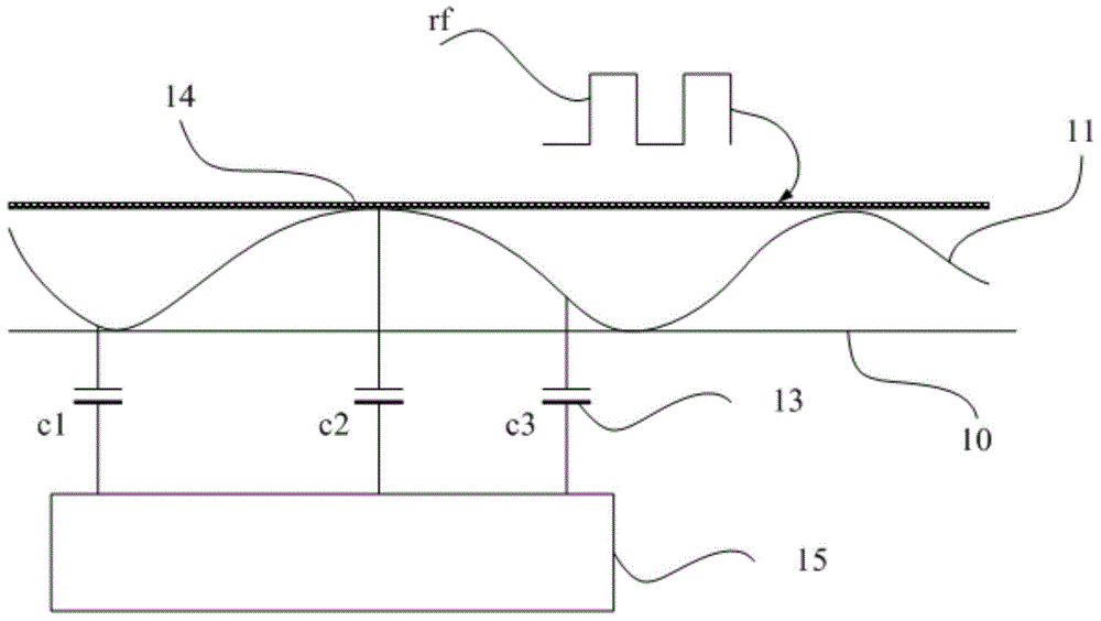
[0064] It can be known from the background art that most of the capacitive fingerprint sensors in the prior art are based on integrated circuits on silicon wafers, which often require a crystalline silicon process, so there are problems of complicated processes and high cost.

[0065] In order to solve the technical problem, the present invention provides a capacitive fingerprint sensor, including:

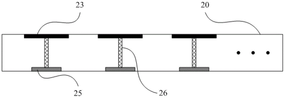
[0066] a substrate; a pixel unit arranged on the surface of the substrate in an array, the pixel unit includes an amorphous switching device, the amorphous switching device includes a control end, a first end and a second end, the first end and the first end The two terminals are turned on or off under the control of the control terminal; the pixel unit further includes a first plate connected to the first terminal of the amorphous switching device, which is used to form a capacitance structure with the fingerprint, and is also used to When the amorphous switching device is turned...


PUM


Abstract

A capacitive fingerprint sensor and a fingerprint imaging module are provided, comprising: a base board; and pixel units that are on a surface of the base board and are arranged in an array, wherein each pixel unit comprises an amorphous switching element and a first pole plate connected to the amorphous switching element, and the first pole plate is used to form a capacitor structure with a fingerprint and output an electrical signal when the amorphous switching element is conducted. According to the invention, the amorphous switching element and the first pole plate connected to the amorphous switching element are arranged, the electrical signal with fingerprint information are obtained by using the first pole plate, and a fingerprint image is obtained according to the electrical signal. The amorphous switching element and the first pole plate are integrated by using an amorphous silicon technology, and a crystalline silicon technology in the prior art is avoided, so that element manufacturing process difficulty can be effectively reduced, process complexity is reduced, an element manufacturing yield is improved, and element manufacturing costs are reduced.

Description

technical field [0001] The invention relates to the field of fingerprint identification, in particular to a capacitive fingerprint sensor and a fingerprint imaging module. Background technique [0002] The fingerprint recognition technology collects the fingerprint image of the human body through the fingerprint sensor, and then compares it with the existing fingerprint imaging information in the fingerprint recognition system to realize the identity recognition. Because fingerprints have the characteristics of lifelong immutability, uniqueness and portability, fingerprint recognition technology has been widely used in various fields, such as: public security bureaus, customs and other security inspection fields, building access control systems, and consumer products such as personal computers and mobile phones. Wait. [0003] The current fingerprint sensors are mainly divided into optical fingerprint sensors and capacitive fingerprint sensors. Among them, the principle of...

Claims


Application Information

Patent Timeline
Patent Type & Authority Applications(China)
IPC IPC(8): G06K9/00
CPCG06V40/1306
Inventor 郑娅洁朱虹凌严
Owner SHANGHAI OXI TECH
Why Eureka
Try Eureka