Shift register unit and driving method thereof, shift register and display device
A shift register and transistor technology, applied in static memory, digital memory information, instruments, etc., can solve the problems of complex structure of shift registers and large space occupied by shift registers, so as to reduce the space occupied and the number of , the effect of simplifying the structure
- Summary
- Abstract
- Description
- Claims
- Application Information
AI Technical Summary
Problems solved by technology
Method used
Image

Examples
Embodiment 1
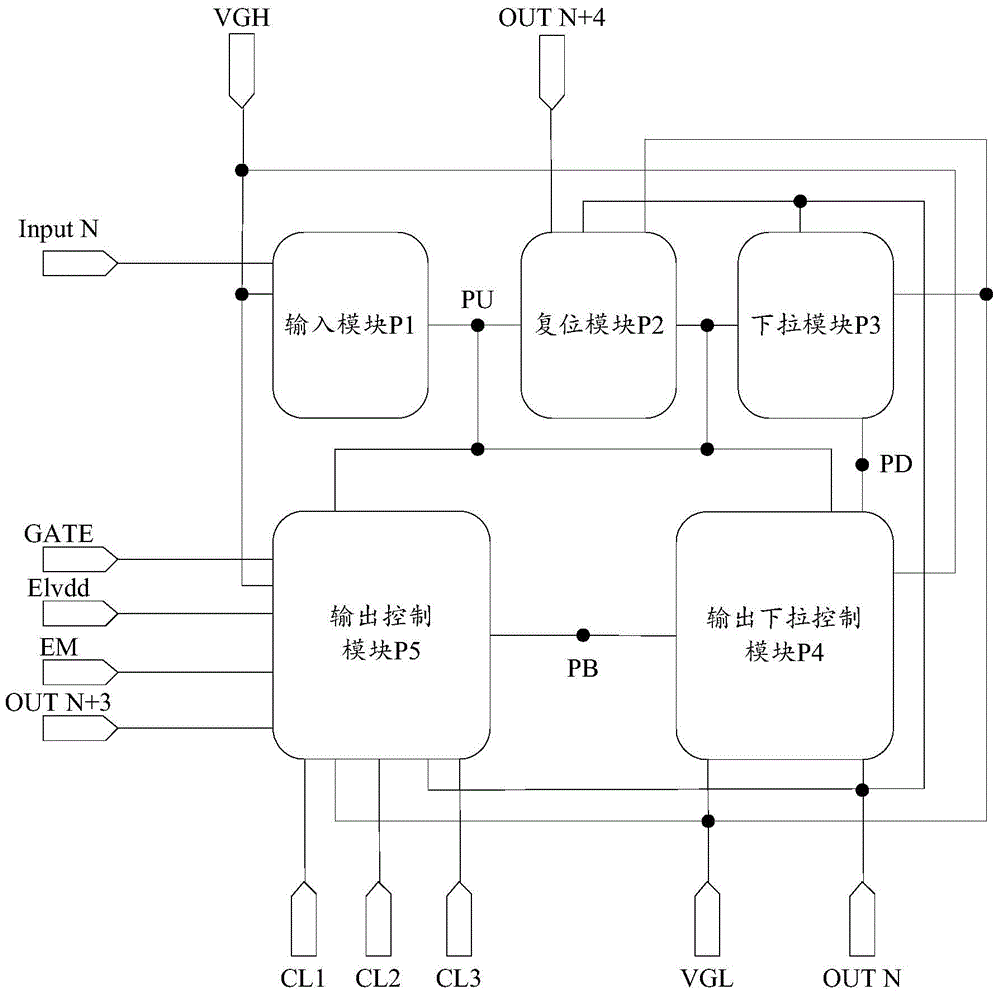
[0026] see figure 1 , the shift register unit provided by the embodiment of the present invention includes an input module P1, a reset module P2, a pull-down module P3, an output pull-down control module P4, and an output control module P5; the Nth-stage shift register unit in the shift register is used for illustration , wherein, the input module P1 is connected to the input signal terminal Input N, the high-level terminal VGH, the pull-up control node PU and the output control module P5, and the pull-up control node PU is the input module P1, the reset module P2, the pull-down module P3, and the output pull-down module The intersection of the control module P4 and the output control module P5, the input module P1 is used to receive the signal of the input signal terminal Input N and the signal of the high level terminal VGH;
[0027] The reset module P2 is connected to the fifth-stage output terminal OUT N+4, the current-stage output terminal OUT N of the shift register unit...
Embodiment 2
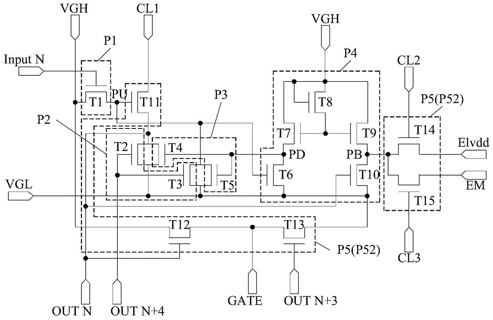
[0037] see figure 2 The specific structures of the input module P1, the reset module P2, the pull-down module P3, the output pull-down control module P4 and the output control module P5 in the first embodiment will be described in detail below.
[0038] The input module P1 includes a first transistor T1, the gate of which is connected to the input signal terminal Input N, the source of which is connected to the high level terminal VGH and the output control module P5, and the drain of which is connected to the pull-up control node PU.
[0039] The reset module P2 includes a second transistor T2 and a third transistor T3; wherein, the gate of the second transistor T2 is connected to the gate of the third transistor T3 and the output terminal OUT N+4 of the fifth stage, and its source is connected to the shift register The output terminal OUT N of the unit, the pull-down module P3, the output pull-down control module P4 and the output control module P5, the drain of which is co...
Embodiment 3
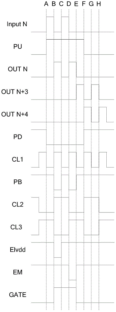
[0055] see Figure 4 , the present invention also provides a kind of shift register, and this shift register comprises the shift register unit in the above-mentioned embodiment 1, 2 of multistage, wherein, the output end of this stage of the shift register unit of the previous stage is connected to the next stage The input signal terminal of the shift register unit. For example, if Figure 4 As shown, the output terminal OUT 1 of the first-stage shift register unit UNIT1 is connected to the input signal terminal Input 2 of the second-stage shift register unit UNIT2.
[0056] Further, the shift register includes N stages of shift register units in the first and second embodiments above, and N is an integer greater than or equal to 4; wherein, the first clock signal terminal CL1 of the i-th shift register unit is connected to The first clock signal terminal CL1 of the shift register unit of the i+2 stage all inputs the first clock signal, and the first clock signal terminal CL...
PUM
 Abstract
Description
Claims
Application Information
 - R&D
- Intellectual Property
- Life Sciences
- Materials
- Tech Scout
- Unparalleled Data Quality
- Higher Quality Content
- 60% Fewer Hallucinations
Browse by: Latest US Patents, China's latest patents, Technical Efficacy Thesaurus, Application Domain, Technology Topic, Popular Technical Reports.
© 2025 PatSnap. All rights reserved.Legal|Privacy policy|Modern Slavery Act Transparency Statement|Sitemap|About US| Contact US: help@patsnap.com