
Drilling method for thick copper circuit board

A technology of thick copper circuit board and production method, which is applied in drilling/drilling equipment, repairing drills, drilling tool accessories, etc., can solve the problems of voids, gaps, copper layer dislocation, etc., so as to increase the bonding area and ensure the adhesion sexual effect

Inactive Publication Date: 2017-12-26
SHENZHEN SUNTAK MULTILAYER PCB
View PDF9 Cites 1 Cited by
  • Summary
  • Abstract
  • Description
  • Claims
  • Application Information

AI Technical Summary

Problems solved by technology

[0004] However, for multi-layer circuit boards designed for thick copper (≥ 3OZ) in the inner layer, the copper thickness is too large, and when the drill bit cuts the copper layer, the drill dirt generated cannot be discharged in time, and the heat generated is too large, and because copper has toughness , copper wire drawing, thermal expansion and deformation in the hole are prone to occur, causing problems such as faults and copper layer misalignment, and the pulling effect of the drill bit on the copper layer causes the copper layer on the inner wall of the hole to shift or create a gap; at the same time, due to heat and impact The action of the force is easy to cause the problem of broken drill bit
In addition, when drilling thick copper plates, it is also prone to the problem of separation between the tin ring of the outer circuit pattern and the substrate, and the prepreg with a resin content of 72% is prone to insufficient resin filling or voids after lamination

Method used


Image

  • Drilling method for thick copper circuit board

Examples


Embodiment

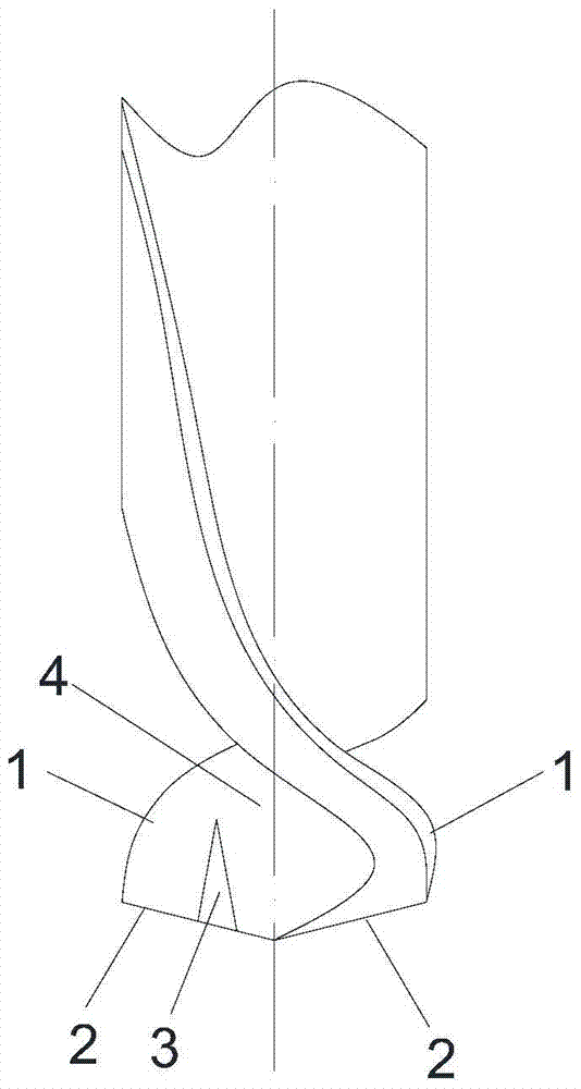
[0023] Such as figure 1 As shown in the drill bit, the drill tip is composed of a drill rod and a drill bit. The drill bit has a diameter of 1.9mm, including a double helix cutting blade 1, and the double helix of the cutting blade 1 forms two helical chip removal grooves 4, the chip removal groove 4 A groove 3 is provided in the axial direction at the drilling end 2 of the drill bit. The groove 3 is triangular in cross section and extends to the drilling end 2 of the drill bit. The groove 3 gradually decreases in axial width and depth from the drilling end 2 of the drill bit. The maximum depth of the groove 3 is 1 / 2 of the thickness of the cutting blade 1 , and the smallest width end is connected with the surface of the cutting blade 1 . The axial angle between the drilling end 2 of the drill bit and the drill bit is 67.5°.

[0024] Use the drill bit above to make circuit board drilling. The circuit board is a laminated board with 6 layers of copper lines. The copper thickn...


PUM

PropertyMeasurementUnit
diameteraaaaaaaaaa
thicknessaaaaaaaaaa

Abstract

The invention discloses a drilling method of a thick copper circuit board and relates to the technical field of circuit board manufacturing. The drilling method uses a drill with the rotation speed of 20-30krmp, tool feeding speed of 20-30mm / s and tool retracting speed of 220-300mm / s to drill holes. The drill comprises a drill stem and a drill bit. The drill bit comprises a cutting blade and a chip groove. The chip groove is axially provided with a groove at the drilling end of the drill bit. The thickness of copper of the inner circuit of the circuit board is not smaller than 3OZ. The method has the advantages that the drill with the groove notch is used, the groove notch in the drilling end of the3 drill bit can cut off a drilling copper wire, the cut-off copper wire can be discharge timely through the groove during drilling, and problems such as hole blocking and drilling copper wire drawing are avoided.

Description

technical field [0001] The invention relates to the technical field of circuit board production, in particular to a drilling method for thick copper circuit boards. Background technique [0002] In the production of circuit boards, prepregs with a resin content of 72% and easy lamination and low cost are generally used. In the outer circuit production process, if there is no special requirement, the diameter of the tin ring is 0.35mm (the tin ring is located on the hole position line The copper ring, the drilling diameter is 1.8mm ~ 1.95mm). Boards for such common designs are usually produced with the following parameters: [0003] Ordinary drill nozzles are used to drill through at one time when drilling, and the speed, feed speed, and retract speed are 35krpm, 36mm / s, and 340mm / s respectively. [0004] However, for multi-layer circuit boards designed for thick copper (≥ 3OZ) in the inner layer, the copper thickness is too large, and when the drill bit cuts the copper lay...

Claims


Application Information

Patent Timeline
Patent Type & Authority Patents(China)
IPC IPC(8): B23B35/00B23B51/00
CPCB23B35/00B23B51/00B23B2251/40
Inventor 王淑怡彭卫红阙玉龙朱拓
Owner SHENZHEN SUNTAK MULTILAYER PCB
Learn More