Semiconductor device and semiconductor device packaging body using the semiconductor device

A semiconductor and packaging technology, which is applied to semiconductor devices, semiconductor/solid-state device components, electric solid-state devices, etc., to achieve the effect of increasing breakdown voltage and reducing parasitic capacitance

Active Publication Date: 2015-09-02
ANCORA SEMICON INC
View PDF3 Cites 5 Cited by
  • Summary
  • Abstract
  • Description
  • Claims
  • Application Information

AI Technical Summary

Problems solved by technology

The drain is on the active layer

Method used


Image

  • Semiconductor device and semiconductor device packaging body using the semiconductor device
  • Semiconductor device and semiconductor device packaging body using the semiconductor device
  • Semiconductor device and semiconductor device packaging body using the semiconductor device

Examples


Embodiment Construction

[0100] Various embodiments of the present invention will be disclosed below with accompanying drawings, and for the sake of clarity, many practical details will be described together in the following description. It should be understood, however, that these practical details should not be used to limit the invention. That is, in some embodiments of the invention, these practical details are unnecessary. In addition, for the purpose of simplifying the drawings, some well-known and conventional structures and elements are shown in a simplified and schematic manner in the drawings.

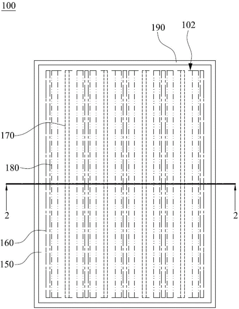
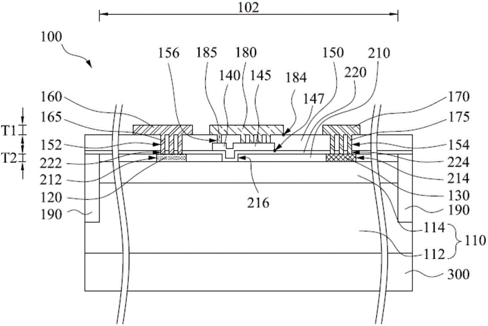
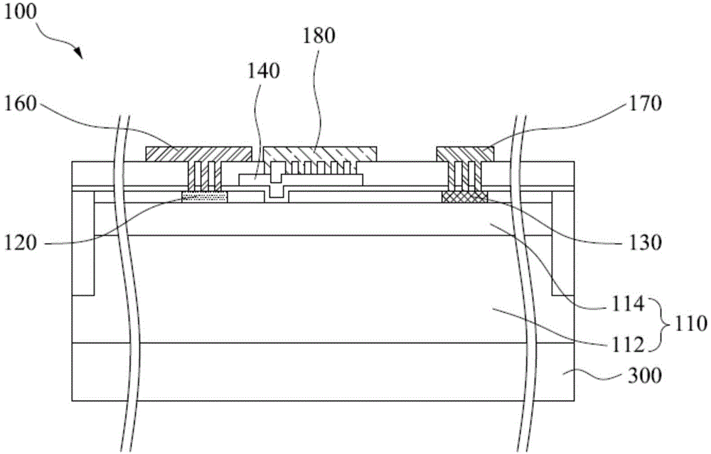
[0101] Please refer to figure 1 and figure 2 ,in figure 1 It is a top view of the semiconductor device 100 according to an embodiment of the present invention, figure 2 for the edge figure 1 A cross-sectional view of line segment 2-2. As shown in the figure, the semiconductor device 100 includes an active layer 110, at least one source electrode 120, at least one drain electrode 130, at least...


PUM


Abstract

A semiconductor device comprises an active layer, a source electrode, a drain electrode, a grid electrode, an interlayer dielectric layer, a source electrode interface layer, at least one inter-source-electrode plug, a drain electrode interface layer, at least one inter-drain-electrode plug, a grid electrode interface layer and at least one inter-grid-electrode plug. The active layer is made of III-V compound semiconductor materials. The source electrode and the drain electrode are located on the active layer. The grid electrode is located on the active layer and arranged between the source electrode and the drain electrode. The interlayer dielectric layer covers the source electrode, the drain electrode and the grid electrode. The source electrode interface layer, the drain electrode interface layer and the grid electrode interface layer are all located on the interlayer dielectric layer. The inter-source-electrode plug is electrically connected with the source electrode and the source electrode interface layer. The inter-drain-electrode plug is electrically connected with the drain electrode and the drain electrode interface layer. The inter-grid-electrode plug is electrically connected with the grid electrode and the grid electrode interface layer. A semiconductor device packaging body using the semiconductor device is also disclosed.

Description

technical field [0001] The present invention relates to a semiconductor device. Background technique [0002] Field Effect Transistor (Field Effect Transistor) is a switching element that utilizes electric field effect in materials to control current, and is widely used in circuits of semiconductor elements. Specifically, the field effect transistor includes a gate electrode, a source electrode, a drain electrode and an active layer, and the source electrode and the drain electrode are respectively located on opposite sides of the active layer. By controlling the voltage of the gate to affect the switching of the channel, a current can be conducted between the source and the drain to be in an on state. [0003] Generally speaking, according to different designs, parasitic capacitances exist inside the field effect transistors, and these parasitic capacitances can degrade the operation characteristics of the field effect transistors. On the other hand, in the packaging stru...

Claims


Application Information

Patent Timeline
IPC IPC(8): H01L29/772H01L29/423H01L23/488
CPCH01L29/2003H01L29/42312H01L29/772H01L29/778H01L23/488H01L2224/0603H01L2224/48137H01L2224/48247H01L2224/48257H01L2224/49111H01L2924/00
Inventor 林立凡杨竣杰廖文甲薛清全陈世鹏
Owner ANCORA SEMICON INC
Why Eureka
Try Eureka