Clock phase control circuit

A technology for controlling circuit and clock phase, applied in the field of clock phase control circuit, can solve the problems of transistor state changing too late, occupying PCB board area, increasing cost, etc., to achieve the effect of reduced clock buffer function, simple circuit principle and easy integration

Inactive Publication Date: 2015-09-02
SHANGHAI BRIGHT POWER SEMICONDUCTOR CO LTD
View PDF3 Cites 2 Cited by
  • Summary
  • Abstract
  • Description
  • Claims
  • Application Information

AI Technical Summary

Problems solved by technology

If the clock frequency is too high, the state of the transistor may not change in time, resulting in deadlock or random misoperation
At the same time, due to the needs of the working state of the circuit, the phase of the clock needs to be adjusted. The existing clock phase adjustment usually relies on a separate chip, which increases the cost and occupies the area of ​​the PCB board.

Method used


Image

  • Clock phase control circuit

Examples


Embodiment Construction

[0012] The specific embodiment of the present invention will be further described in detail below in conjunction with the accompanying drawings.

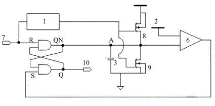
[0013] The clock phase control circuit of the present invention comprises a clock input stage, a capacitor 3, a level detection circuit 6, a pull-up circuit 8, a pull-down circuit 9, a clock output stage and a logic control circuit 1, the output terminal of the clock input stage and the level detection circuit The input terminal of circuit 6 is connected to point A, and point A is also connected to the output terminals of capacitor 3, pull-up circuit 8 and pull-down circuit 9, and the other end of the capacitor is connected to a fixed DC level, preferably grounded; said level detection circuit 6 The voltage at point A is detected, and the detection signal is output to the clock output stage; the logic control circuit 1 is connected with the clock input stage, the pull-up circuit 8 and the pull-down circuit 9, and controls the pull-up...


PUM


Abstract

A clock phase control circuit comprises a clock input stage, a capacitor, a level detection circuit, a pull-up circuit, a pull-down circuit, a clock output stage and a logic control circuit. The output end of the clock input stage and the input end of the level detection circuit are connected at an A point, and the A point is also connected with the output ends of the capacitor, the pull-up circuit and the pull-down circuit. The other end of the capacitor is connected with a fixed DC level, and the level detection circuit detects the voltage of the A point and outputs a detection signal to the clock output stage. The logic control circuit is connected with the clock input stage, the pull-up circuit and the pull-down circuit, and controls the pull-up circuit and the pull-down circuit to be turned on at the high level time and the low level time of a clock respectively. The clock phase control circuit of the present invention starts to charge and discharge the capacitor at the rising or falling edge of the clock, thereby causing the time delay of a signal output edge. The clock phase control circuit is simple in circuit principle, is convenient to integrate in an integrated circuit existing technology, does not need to the support of a peripheral separating electronic component, realizes a clock buffer function, and also enables the circuit cost to be reduced.

Description

technical field [0001] The invention belongs to the field of electronic circuits and relates to a clock phase control circuit. Background technique [0002] The clock frequency refers to the basic frequency of the clock in the synchronous circuit, which is measured by "several cycles per second", and the measurement unit is the SI unit hertz (Hz). Numerous transistors in digital circuits and analog circuit chips all work in the switch state, and their conduction and shutdown actions are all carried out in accordance with the rhythm of the clock signal. If the clock frequency is too high, the state of the transistor may not change in time, resulting in deadlock or random misoperation. At the same time, due to the needs of the working state of the circuit, the phase of the clock needs to be adjusted. The existing clock phase adjustment usually relies on a separate chip, which increases the cost and occupies the area of ​​the PCB board. Contents of the invention [0003] In...

Claims


Application Information

Patent Timeline
IPC IPC(8): H03K5/13
Inventor 高继赵方麟易坤陈雪松
Owner SHANGHAI BRIGHT POWER SEMICONDUCTOR CO LTD
Why Eureka
Try Eureka