Power module

A power module and power cycle technology, applied in semiconductor/solid-state device parts, welding equipment, manufacturing tools, etc., can solve problems such as thermal resistance rise, solder cracking, etc., to achieve improved reliability, high reliability, and sufficient reliability. sexual effect

Active Publication Date: 2015-09-02
MITSUBISHI MATERIALS CORP
View PDF5 Cites 7 Cited by
  • Summary
  • Abstract
  • Description
  • Claims
  • Application Information

AI Technical Summary

Problems solved by technology

[0011] However, as described in Patent Document 3, for example, if a power cycle load is applied to a power module in which a Ni plating layer is formed on the surface of a circuit layer made of aluminum or an aluminum alloy and a semiconductor element is solder-bonded, torsion may occur on the solder. crack, the thermal resistance will rise
[0012] Also, even in a power module in which a Ni plating layer is formed on the surface of a circuit layer made of copper or copper alloy and semiconductor elements are soldered together, if a power cycle load is applied, cracks may also occur on the solder and the thermal resistance will increase.

Method used


Image

  • Power module
  • Power module
  • Power module

Examples


no. 1 Embodiment approach

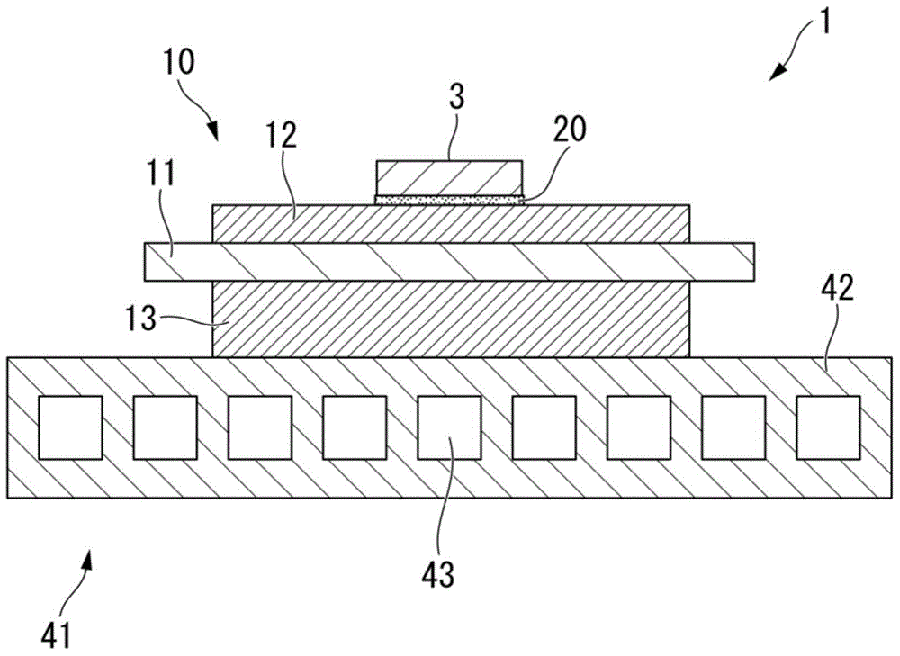
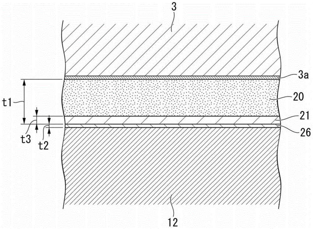
[0037] figure 1 The power module 1 according to the first embodiment of the present invention is shown in . This power module 1 includes a power module substrate 10 in which a circuit layer 12 is disposed on one surface (first surface) of an insulating substrate (insulating layer) 11, and a power module mounted on the circuit layer 12 ( figure 1 The middle is the upper surface) of the semiconductor element 3 . In addition, in the power module 1 of the present embodiment, the heat sink 41 is bonded to the other surface side (the second surface side, the second surface side) of the insulating substrate 11 . figure 1 middle is the lower surface).

[0038] The power module substrate 10 includes: an insulating substrate 11 constituting an insulating layer; figure 1 and the circuit layer 12 arranged on the other side of the insulating substrate 11 (being the second side, figure 1 The middle is the metal layer 13 of the lower surface).

[0039] The insulating substrate 11 is a s...

no. 2 Embodiment approach

[0069] Next, a power module according to a second embodiment of the present invention will be described with reference to the drawings. In addition, the same code|symbol is attached|subjected to the same member as 1st Embodiment, and detailed description is abbreviate|omitted.

[0070] Figure 5 A power module 101 according to the second embodiment of the present invention is shown in . This power module 101 includes a power module substrate 110 in which a circuit layer 112 is formed on one surface (first surface) of an insulating substrate (insulating layer) 11, and a substrate mounted on the circuit layer 112 ( Figure 5 The middle is the upper surface) of the semiconductor element 3 .

[0071] The power module substrate 110 includes: an insulating substrate 11 constituting an insulating layer; Figure 5 and the circuit layer 112 arranged on the other side of the insulating substrate 11 (being the second side, Figure 5 The middle is the metal layer 13 of the lower surfa...

Embodiment 1

[0114]Hereinafter, the results of confirmation experiments conducted to confirm the effects of the present invention will be described.

[0115] The power module described in the first embodiment is prepared. The insulating substrate is made of AlN, and a substrate with a size of 27 mm×17 mm and a thickness of 0.6 mm is used. In addition, the circuit layer was made of oxygen-free copper, and a layer of 25 mm×15 mm and a thickness of 0.3 mm was used. The metal layer is made of 4N aluminum, and a layer of 25 mm×15 mm and a thickness of 0.6 mm is used. The semiconductor element was an IGBT element, and an element with a size of 13 mm×10 mm and a thickness of 0.25 mm was used. An aluminum plate (A6063) of 40.0 mm x 40.0 mm x 2.5 mm was used as the heat sink.

[0116] Here, the thickness of the Ni plating film formed on the surface of the circuit layer was adjusted, and the composition of the solder material was changed as shown in Table 1, thereby adjusting the composition of t...


PUM

PropertyMeasurementUnit
thicknessaaaaaaaaaa
thicknessaaaaaaaaaa
thicknessaaaaaaaaaa

Abstract

This power module has: a copper layer comprising copper or a copper alloy, provided on a circuit layer (12) surface bonded to a semiconductor element (3); and a soldered layer (20) formed by using a solder material and formed between the circuit layer (12) and the semiconductor element (3). An alloy layer (21) containing Sn as the main component thereof and also containing 0.5-10 mass% Ni and 30-40 mass% Cu is formed in the interface between the soldered layer (20) and the circuit layer (12). The thickness of this alloy layer (21) is set in the range of 2-20 µm, and has a thermal resistance increase rate of no more than 10% in a power cycle test in which the power cycle under conditions of a temperature difference of 80°C and a conduction duration of 5 s is set to a load of 100,000 times.

Description

technical field [0001] The present invention relates to a power module in which a circuit layer provided with a copper layer made of copper or a copper alloy is bonded to a semiconductor element using a solder material. [0002] This application claims priority based on Patent Application No. 2012-281346 for which it applied in Japan on December 25, 2012, and uses the content here. Background technique [0003] For example, as shown in Patent Documents 1 and 2, the power module includes a power module substrate formed by bonding a metal plate as a circuit layer to one surface of an insulating substrate, and a power element (semiconductor element) mounted on the circuit layer. [0004] In addition, a radiator such as a radiator plate or a cooler may be arranged on the other surface side of the power module substrate to dissipate heat from the power element (semiconductor element). At this time, in order to relax the thermal stress caused by the thermal expansion coefficient ...

Claims


Application Information

Patent Timeline
Patent Type & Authority Applications(China)
IPC IPC(8): H01L21/52B23K35/26C22C13/00
CPCC22C13/00H01L23/473H01L24/29H01L2224/29111H01L2224/32503H01L23/3107H01L24/32H01L2224/29005H01L2924/01322H01L2224/32238H01L2224/83801H01L2224/32507H01L2924/3512H01L23/3735B23K35/26H01L2924/13055H01L23/488H01L21/52H01L2224/83447H01L2924/00H01L2924/206H01L2924/01029H01L2924/01028H01L2924/00014B23K35/262B23K35/0222B23K35/0238H05K7/02
Inventor 大桥东洋长友义幸长瀬敏之黑光祥郎
Owner MITSUBISHI MATERIALS CORP
Why Eureka
Try Eureka