

Chip positioning clamp of vacuum eutectic soldering, manufacturing method and chip transferring method
A positioning fixture and eutectic welding technology, applied in semiconductor/solid-state device manufacturing, electrical components, circuits, etc., can solve problems such as affecting microwave power, and achieve the effects of improving position accuracy, reducing process time, and not easily deformed
- Summary
- Abstract
- Description
- Claims
- Application Information
AI Technical Summary
Problems solved by technology
Method used
Image

Examples
Embodiment 1
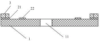
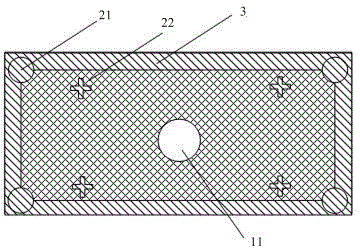
[0059] combine figure 1 - Fig. 4, this embodiment describes in detail the positioning fixture of the vacuum eutectic welding of the present invention, as figure 1 Shown is a cutaway view of the positioning fixture, as figure 2It is shown in a top view, which includes: a substrate 1, a support step 2 and a limit step 3, wherein: the substrate 1 is provided with an adsorption hole 11 for absorbing chips; the support step 2 is located on the surface area of the substrate, and For supporting the chip; the limit step 3 is located on the surface area of the support step away from the substrate, and is used to limit the movement of the chip.
[0060] The positioning fixture of this embodiment is a positioning fixture for GaAs bare chips, the substrate 1 is a rectangular ceramic sheet slightly larger than the chip, and the adsorption hole 11 is located at the center of the substrate 1; the supporting step 2 includes a first frame 21 and an island 22 , the first frame 21 is a ...
Embodiment 2
[0064] combine Figure 5 - Fig. 6, this embodiment describes in detail the manufacturing method of the chip positioning jig of the present invention, as Figure 5 shown, which includes the following steps:
[0065] S71: forming a support step on the surface of the substrate;
[0066] S72: forming a limit step on the support step;
[0067] S73: Machining an adsorption hole at the center of the substrate.
[0068] Wherein: Step S71 further includes:
[0069] S711: Provide a substrate, clean one surface, and sputter a layer of copper seed layer, and the cross-sectional view of the corresponding positioning fixture is as follows Figure 6A shown;
[0070] S712: An electroformed mask for supporting steps is formed on the surface of the copper seed layer by photolithography with SU8 glue, and the sectional view of the corresponding positioning fixture is as follows Figure 6B shown;
[0071] S713: Nickel is electroformed on the surface of the copper seed layer to form the fir...
Embodiment 3
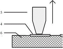
[0079] combine Figure 7 , this embodiment describes in detail the chip transfer method of the present invention, which includes the following steps:
[0080] S111: the suction head sucks the chip positioning fixture;
[0081] S112: the suction head adsorbs the chip on the limit step of the chip positioning fixture through the adsorption hole;
[0082] S113: moving the chip to a suitable position in the packaging box;
[0083] S114: Remove the suction head, and install a pressure rod above the substrate of the chip positioning jig.
PUM
| Property | Measurement | Unit |
|---|---|---|
| Thickness | aaaaa | aaaaa |
Abstract
Description
Claims
Application Information