Method of forming semiconductor device

A semiconductor and device technology, applied in the field of semiconductor device formation, can solve the problems of semiconductor device quality and reliability degradation, easy to appear holes, etc.

Active Publication Date: 2018-05-01
SEMICON MFG INT (SHANGHAI) CORP +1
View PDF3 Cites 0 Cited by
  • Summary
  • Abstract
  • Description
  • Claims
  • Application Information

AI Technical Summary

Problems solved by technology

This overhang phenomenon leads to the formation of plugs, the interlayer dielectric layer near the plugs is prone to voids, resulting in a decline in the quality and reliability of semiconductor devices.
[0010] Therefore, a new method of forming a semiconductor device is needed to prevent the overhanging phenomenon of the plug during the formation of the semiconductor device, thereby preventing holes in the interlayer dielectric layer near the plug, thereby preventing the quality and reliability of the semiconductor device from declining

Method used


Image

  • Method of forming semiconductor device
  • Method of forming semiconductor device
  • Method of forming semiconductor device

Examples


Embodiment Construction

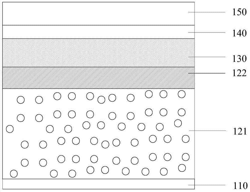
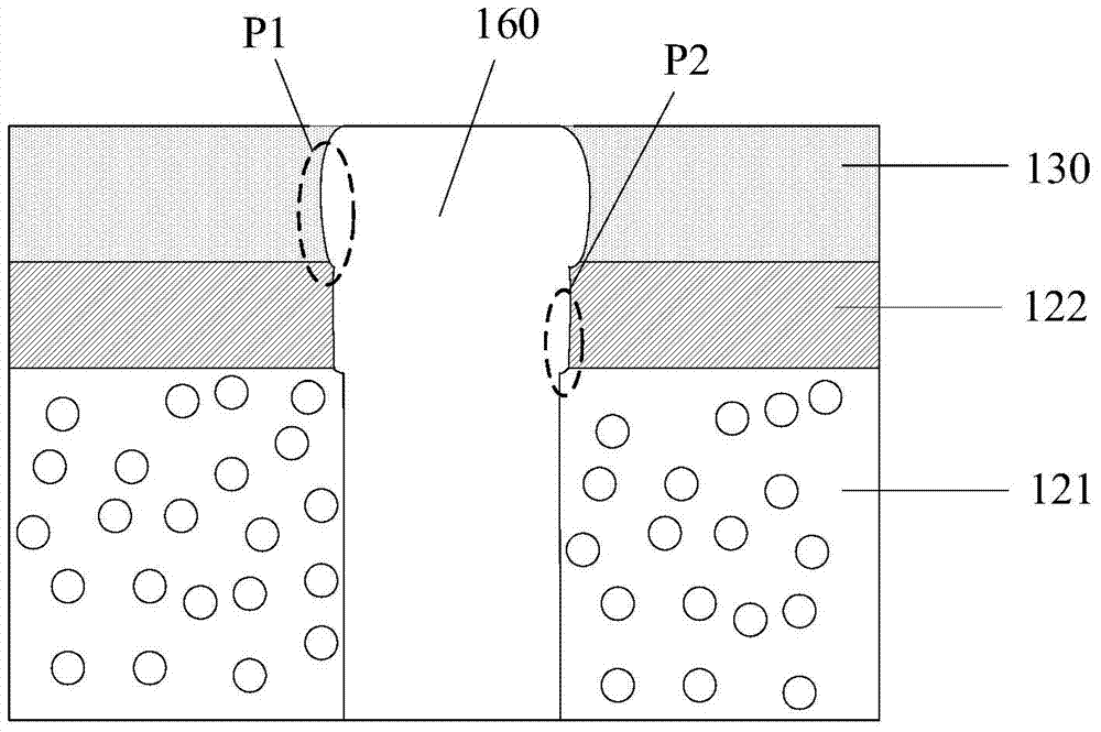
[0032] As mentioned in the background, in the formation process of existing semiconductor devices, there is a problem that plugs are prone to overhang in each stacked structure.

[0033] After research, it was found that the reason for the overhang phenomenon is that after the via holes are formed in the stacked structure (including the etch stop layer, the first low-K dielectric layer, the second low-K dielectric layer and the hard mask layer), it is necessary to The through holes are cleaned by using an acid solution, that is, the through holes are subjected to a pickling process. During the pickling process, the acid solution has a certain etching effect on the first low-K dielectric layer, the second low-K dielectric layer and the hard mask layer, and the acid solution has a certain etching effect on the first low-K dielectric layer and the second low-K dielectric layer. and the etching rate of the hard mask layer increase sequentially, resulting in that after cleaning, th...


PUM


Abstract

Provided is a semiconductor device forming method which comprises: providing a semiconductor substrate; forming a first low-K dielectric layer on the semiconductor substrate; forming a second low-K dielectric layer on the first low-K dielectric layer; and performing ultraviolet irradiation on the second low-K dielectric layer. The forming method may improve the quality and the reliability of a semiconductor device.

Description

technical field [0001] The invention relates to the field of semiconductor manufacturing, in particular to a method for forming a semiconductor device. Background technique [0002] With the development of semiconductor technology, integrated circuits are developing in the direction of high integration. The requirement of high integration makes the line width of the semiconductor structure smaller and smaller, and the reduction of the line width puts forward higher requirements for the formation process of the integrated circuit. [0003] In a semiconductor structure, a semiconductor device is usually formed by a multilayer metal layer and a multilayer interlayer dielectric layer, etc., and the multilayer metal layer is electrically connected by a plug disposed in the interlayer dielectric layer. As the line width decreases, low-K dielectric layers have been widely used as interlayer dielectric layers. [0004] In the prior art, after forming the low-K dielectric layer, a ...

Claims


Application Information

Patent Timeline
Patent Type & Authority Patents(China)
IPC IPC(8): H01L21/768
CPCH01L21/76825H01L21/76835
Inventor 周鸣
Owner SEMICON MFG INT (SHANGHAI) CORP
Why Eureka
Try Eureka