Device for switching waveguide to substrate integrated waveguide

A substrate-integrated waveguide and conversion device technology, applied in connection devices, waveguide-type devices, electrical components, etc., can solve the design and test obstacles of substrate-integrated waveguide circuits, coaxial cables are susceptible to interference, and coaxial connectors are expensive, etc. problems, to achieve the effect of small processing difficulty, low processing cost, simple and compact structure

Inactive Publication Date: 2015-09-09
SOUTHEAST UNIV
View PDF1 Cites 20 Cited by
  • Summary
  • Abstract
  • Description
  • Claims
  • Application Information

AI Technical Summary

Problems solved by technology

However, for frequency bands above 50GHz, coaxial connectors are particularly expensive, and coaxial connectors and coaxial cables are particularly susceptible to interference in such high frequency bands, and performance degradation is very serious. Therefore, people usually use traditional metal waveguides for connection and testing
The c...

Method used


Image

  • Device for switching waveguide to substrate integrated waveguide
  • Device for switching waveguide to substrate integrated waveguide
  • Device for switching waveguide to substrate integrated waveguide

Examples


example

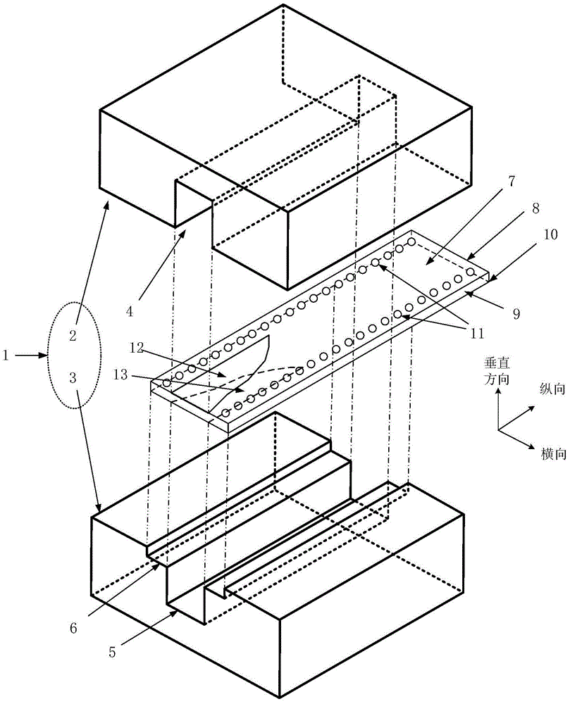
[0062] The structure of the conversion device from the waveguide to the substrate-integrated waveguide applicable to the V-band, that is, 50GHz-75GHz, is shown in the figure. In order to facilitate testing, this example adopts a back-to-back structure, that is, a waveguide-substrate integrated waveguide-waveguide conversion device is designed.

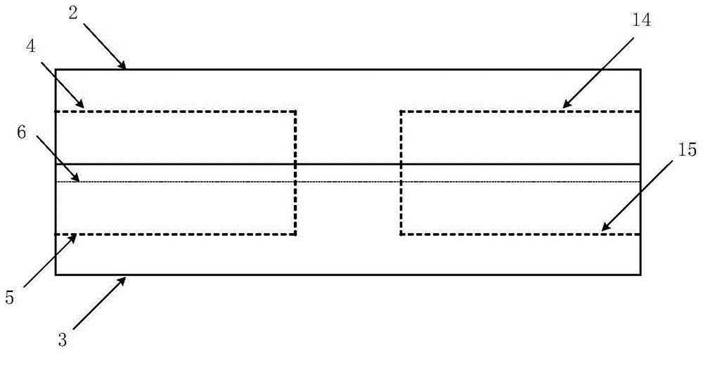
[0063] The size of the upper metal block 2 and the lower metal block 3 of the special waveguide 1 is 22.0mm×30.0mm×10.0mm, and the material is copper, and the size of the substrate groove 6 is 11.0mm×30.0mm×0.28mm; the waveguide of the special waveguide 1 The total size of the mouth is 1.88mm×9.0mm×3.759m; the distance between the centerlines of the two rows of metallized through-hole columns of the substrate integrated waveguide 7 is 2.814mm, the distance between the centers of adjacent through-holes is 0.6mm, and the diameter of the through-holes The thickness of the top metal layer 8 and the bottom metal layer 10 are both 0.018mm; t...


PUM

PropertyMeasurementUnit
Diameteraaaaaaaaaa

Abstract

The invention discloses a device for switching a waveguide to a substrate integrated waveguide. The device comprises a special waveguide and a substrate integrated waveguide; the substrate integrated waveguide consists of a top metal layer, a dielectric substrate and a bottom metal layer; the top metal layer is etched with first multi-folding fin line gaps; the bottom metal layer is etched with second multi-folding fin line gaps; the special waveguide comprises an upper metal block and a lower metal block, the upper metal block is provided with a first waveguide slot, and the lower metal block is provided with a second waveguide slot and a substrate slot; the substrate integrated waveguide is put into the substrate slot, the first multi-folding fin line gaps are matched and aligned with the first waveguide slot, and the second multi-folding fin line gaps are matched and aligned with the second waveguide slot; and the first waveguide slot and the second waveguide slot form a waveguide opening of a standard waveguide. The device has the advantages of wide band, low insertion loss, low reflection coefficient, low machining cost, low machining difficulty and small size, so the device is favorable for large-scale production and application.

Description

technical field [0001] The invention relates to a conversion device from a waveguide to a substrate integrated waveguide formed by connecting a special waveguide with a substrate integrated waveguide etched with multi-fold fin line gaps on the surface, belonging to the technical field of microwave and millimeter wave devices. Background technique [0002] In the microwave wireless communication system, the microwave circuit has always been a very important basic hardware, so it has received great attention from people. At the end of the 19th century, the development of electromagnetic field and electromagnetic wave theory gave birth to the basic concept of microwave circuits, and the guided wave structure is the basis of microwave circuits, which is related to the overall performance of microwave systems. With the development of guided wave structures until the beginning of the 21st century, researchers proposed low-loss, easy-to-integrate, and miniaturized substrate-integra...

Claims


Application Information

Patent Timeline
IPC IPC(8): H01P5/08
Inventor 陈继新彭小莹洪伟汤红军严蘋蘋候德彬张慧
Owner SOUTHEAST UNIV
Why Eureka
Try Eureka