Circuit for reducing residual offset of integrated hall sensor

A Hall sensor and residual technology, applied in the direction of adjusting electrical variables, using electrical/magnetic devices to transmit sensing components, instruments, etc., can solve the problem of not effectively eliminating package stress and junction field effect imbalance, signal conditioning circuit residual imbalance elimination, Large residual offset and other problems, to achieve the effect of easy circuit integration, elimination of offset, and low residual offset

Active Publication Date: 2015-09-23
南京奇霍科技有限公司
View PDF4 Cites 7 Cited by
  • Summary
  • Abstract
  • Description
  • Claims
  • Application Information

AI Technical Summary

Problems solved by technology

At present, the dynamic offset cancellation technology of two-phase rotating current is used to eliminate Hall offset, but it cannot effectively eliminate the offset caused by package stress and junction field effect, so the residual offset is relatively large
On the other hand, the signal conditioning circuit that eliminates the offset and amplifies the Hall signal, including the amplifier, demodulator, sample and hold circuit itself also has a large offset voltage, especially the demodulator recovers the high-frequency signal modulated by the rotating current In the process of reaching the low frequency signal, due to the non-ideal type of the switch in the circuit, it also causes a large residual offset
However, there is no good way to eliminate the residual offset caused by the signal conditioning circuit

Method used


Image

  • Circuit for reducing residual offset of integrated hall sensor
  • Circuit for reducing residual offset of integrated hall sensor
  • Circuit for reducing residual offset of integrated hall sensor

Examples


Embodiment Construction

[0025] In order to make the object, technical solution and advantages of the present invention clearer, the present invention will be further described in detail below in conjunction with the accompanying drawings and embodiments. It should be understood that the specific embodiments described here are only used to explain the present invention, not to limit the present invention.

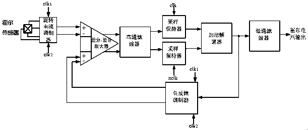
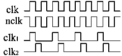
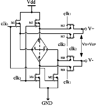
[0026] Such as figure 1 , the Hall sensor modulates the Hall signal into a high-frequency signal through a two-phase rotating current modulator, while the polarity of the offset signal remains unchanged, so that the Hall signal can be distinguished from the offset signal. The output of the rotating current modulator is mixed with the offset Hall signal and sent to a pair of input ports of the differential-differential amplifier, while the output signal of the Hall sensor is sent to the other pair of differential-differential amplifier through the negative feedback modulator output feedback signal ...


PUM


Abstract

The invention discloses a circuit for reducing the residual offset of an integrated hall sensor. The circuit employs rotating current modulation and high-pass filtering, and enables offset and low-frequency 1/f noise, which are generated by a hall device, to be eliminated in advance, and then further eliminates hall offset through a subsequent demodulation circuit. Therefore, the circuit is stronger in capability of eliminating the hall device offset. A signal demodulated by the hall sensor is enabled to be modulated into a high-frequency signal through a feedback modulator, and the high-frequency signal serves as a feedback signal and is transmitted to a difference-difference amplifier for amplification along with a hall signal outputted by a rotating current modulator, thereby forming a closed-loop signal conditioning circuit, and further reducing the residual offset caused by the signal conditioning circuit. The circuit is simple in structure, is easy to achieve circuit integration, cannot increase the manufacture cost, and can obtain low residual offset.

Description

technical field [0001] The invention relates to a signal processing circuit, in particular to a circuit for reducing the residual offset of an integrated Hall sensor. Background technique [0002] The Hall sensor is a magnetoelectric conversion element based on the Hall effect. With its simple process, small size, low production cost, easy installation, wide operating voltage range, long service life, high measurement accuracy, dust-proof, oil-proof, etc. Advantages, has been widely used in industrial frequency conversion control, transportation, medical systems, consumer electronics and various smart instruments and other fields. [0003] However, the integrated Hall sensor based on the silicon process has low magnetic field sensitivity and serious offset, so the weak Hall signal must be amplified and the offset signal eliminated through the corresponding signal conditioning circuit. However, the Hall signal output by the Hall sensor still carries a large residual offset, ...

Claims


Application Information

Patent Timeline
Patent Type & Authority Applications(China)
IPC IPC(8): G01D5/14G05F1/56
Inventor 徐跃郑文添欧思维赵银泽
Owner 南京奇霍科技有限公司
Why Eureka
Try Eureka