On-chip Hall Signal Amplifier and Method Based on Chopper Second-Order Compensation

A Hall signal, second-order compensation technology, applied in amplifiers, amplifiers with semiconductor devices/discharge tubes, improving amplifiers to reduce temperature/power supply voltage changes, etc. Good and other problems, to achieve the effect of cost increase and linearity improvement

Active Publication Date: 2020-12-15
NINGBO CRRC TIMES TRANSDUCER TECH CO LTD
View PDF0 Cites 0 Cited by
  • Summary
  • Abstract
  • Description
  • Claims
  • Application Information

AI Technical Summary

Problems solved by technology

[0002] In the design of integrated circuits, there are often problems such as operational amplifier misalignment, excessive voltage, excessive device temperature drift, and poor linearity characteristics during small signal amplification.
[0003] In order to solve the above problems, technicians often need to do zero drift, temperature drift elimination, and linearity compensation for the signal conditioning amplifier circuit. The problem is that the characteristics of the tubes at the forward and reverse ends of the operational amplifier are inconsistent, and the voltage is out of balance during static operation. If the silicon-based Hall signal is directly amplified, the weak signal is easily overwhelmed by the offset voltage, resulting in signal Extraction is difficult; although adding offset compensation can eliminate the influence of offset voltage in a specific temperature environment and achieve the purpose of zero adjustment, when the temperature changes, the fixed compensation cannot adapt to the temperature change characteristics of the tube, which will also cause the offset compensation to lose its original function. effect
[0004] In addition, due to the silicon-based Hall's sensitivity to the magnetic field will change greatly under different voltages and temperatures, showing nonlinearity, which also makes the linear compensation effect not good.

Method used


Image

  • On-chip Hall Signal Amplifier and Method Based on Chopper Second-Order Compensation
  • On-chip Hall Signal Amplifier and Method Based on Chopper Second-Order Compensation

Examples


Embodiment Construction

[0032] The present invention will be further described in detail below in conjunction with the accompanying drawings and embodiments.

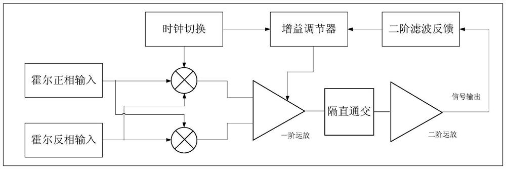
[0033] Such as figure 1 Shown is an on-chip Hall signal amplifier based on chopper second-order compensation, including:

[0034] The signal input module provides the Hall positive-phase input signal and negative-phase input signal to the chopper modulation module;

[0035] The chopping modulation module is connected to the two output terminals of the signal input module, and modulates and outputs the positive-phase input signal and the negative-phase input signal; the chopping modulation module is composed of two mixers;

[0036] The clock module provides switching frequency and modulation frequency for the chopping modulation module; the chopping modulation module switches the input signal between positive phase and negative phase based on the switching frequency of the clock module, and modulates the offset voltage in the input signal to ...


PUM


Abstract

An on-chip Hall signal amplifier based on chopper second-order compensation, comprising: a signal input module for providing a Hall non-inverting input signal and an inverting input signal; a chopper connected to two output terminals of the signal input module A wave modulation module, configured to modulate and output the positive-phase input signal and the reverse-phase input signal; a clock module, used to provide switching frequency and modulation frequency for the chopping modulation module; and the chopping modulation module The op-amp module connected to the two output terminals is used to amplify the output signal of the chopper modulation module; it also includes a second-order compensation module connected to the output terminal of the op-amp module and a clock module, which is used to adjust the op-amp The output signal of the module is compensated and fed back to the inverting input terminal of the operational amplifier module. Compared with the prior art, the invention can effectively eliminate the offset in the whole temperature range, and improve the linearity of the output signal through the second-order compensation.

Description

technical field [0001] The invention relates to the field of signal amplification, in particular to an on-chip Hall signal amplifier based on chopper second-order compensation and methods for eliminating offset and linear compensation. Background technique [0002] In the design of integrated circuits, there are often problems such as operational amplifier misalignment, excessive voltage, excessive temperature drift of devices, and poor linearity characteristics during small signal amplification. [0003] In order to solve the above problems, technicians often need to do zero drift, temperature drift elimination, and linearity compensation for the signal conditioning amplifier circuit. The problem is that the characteristics of the tubes at the forward and reverse ends of the operational amplifier are inconsistent, and the voltage is out of balance during static operation. If the silicon-based Hall signal is directly amplified, the weak signal is easily overwhelmed by the of...

Claims


Application Information

Patent Timeline
Patent Type & Authority Patents(China)
IPC IPC(8): H03F1/30H03F3/387
CPCH03F1/30H03F3/387
Inventor 曹力倪大成王飞郑良广张坡
Owner NINGBO CRRC TIMES TRANSDUCER TECH CO LTD
Why Eureka
Try Eureka