
Dielectric composition and electronic component
A dielectric composition, technology of group A, applied in the direction of fixed capacitance components, inorganic insulators, laminated capacitors, etc., can solve the problems of increasing electrostatic capacitance, film capacitors can not be said to be good for high voltage resistance, etc., to achieve Effect of High Withstand Voltage
- Summary
- Abstract
- Description
- Claims
- Application Information
AI Technical Summary
Problems solved by technology
Method used
Image

Examples
Embodiment 1
[0062]
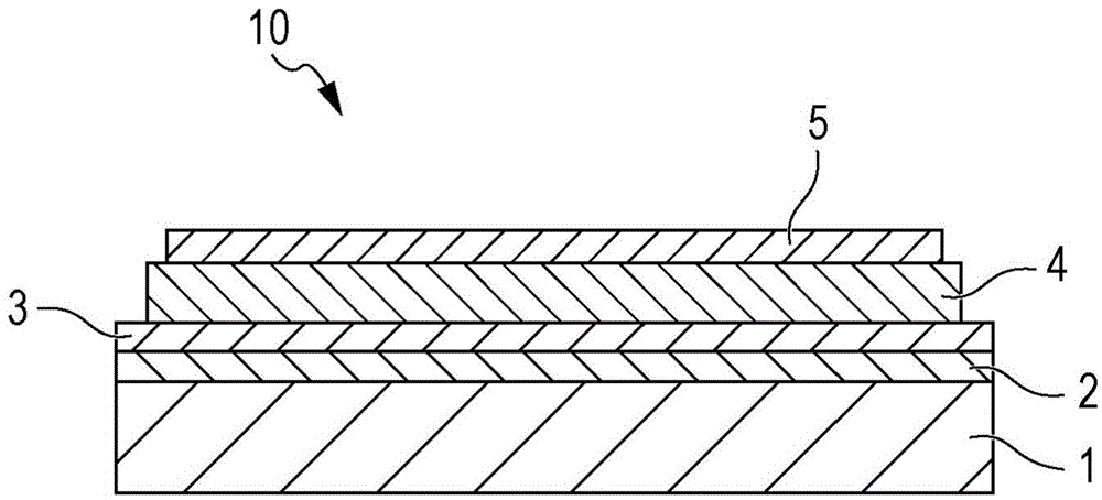
[0063] First, 6 μm SiO is provided on the surface of 350 μm Si 2 On the surface of the 10 mm×10 mm square support substrate of the insulating film, a Ti thin film as an underlayer was formed to have a thickness of 20 nm by a sputtering method.
[0064] Next, a Pt thin film as a lower electrode was formed on the Ti thin film formed above by sputtering so as to have a thickness of 100 nm.
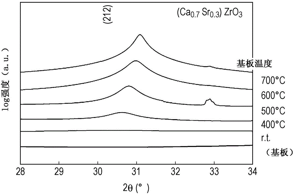
[0065] With respect to the formed Ti / Pt thin film, heat treatment was performed under normal pressure at a heating rate of 400° C. / min, a holding temperature of 700° C., a temperature holding time of 30 minutes, and an oxygen atmosphere.
[0066] The PLD method is used for the formation of the dielectric film. The targets required for forming the dielectric film were produced as follows.
[0067] First, BaCO was carried out so that the ratio of the amounts of Ba, Ca, and Sr in Sample No. 1 to Sample No. 14 and the molar ratio α between Group A and Group B became the values sho...
Embodiment 2
[0090]
[0091] BaCO was carried out so that the ratio of the amount of Ba, Ca, and Sr in sample No. 15 to sample No. 20 and the molar ratio α between group A and group B became the values shown in Table 2. 3 , CaCO 3 , SrCO 3 , ZrO 2 、TiO 2 Weighing, making targets. Film capacitor samples of sample Nos. 15 to 20 were produced in the same manner as in Example 1 except for the composition of the target, and the same evaluations as in Example 1 were performed. The results are shown in Table 2.
[0092] [Table 2]
[0093]
[0094] Sample No.11, Sample No.15~Sample No.18
[0095] According to Table 2, when the molar ratio α of group A and group B is in the range of 0.5≤α≤1.5, and the amorphous and crystalline are in a mixed state, it can be confirmed that the withstand voltage is above 5.0MV / cm, and the relative dielectric constant is over 30.
[0096] Sample No.19, Sample No.20
[0097] According to Table 2, when the molar ratio α of Group A to Group B is α1.5, c...
Embodiment 3
[0098]
[0099] The ratio of the amounts of Ba, Ca, and Sr, the ratio of the amounts of Zr and Ti, and the molar ratio α between the A group and the B group of samples No. 21 to No. 25 were set to the values shown in Table 3. BaCO 3 , CaCO 3 , SrCO 3 , ZrO 2 、TiO 2 Weighing, making targets. Film capacitor samples of sample No. 21 to sample No. 25 were produced in the same manner as in Example 1 except for the composition of the target, and the same evaluations as in Example 1 were performed. The results are shown in Table 3.
[0100] [table 3]
[0101]
[0102] Sample No.11, Sample No.21~Sample No.23
[0103] According to Table 3, in the dielectric composition composed of amorphous containing group A and group B and crystal containing group A and group B, group B containing Zr element also contains Ti element, and the ratio (w) of Ti is 0mol%<w≤60mol%, and when the amorphous and crystalline are in a mixed state, it can be confirmed that the relative permittivit...
PUM
| Property | Measurement | Unit |
|---|---|---|
| coating thickness | aaaaa | aaaaa |
| relative permittivity | aaaaa | aaaaa |
| relative permittivity | aaaaa | aaaaa |
Abstract
Description
Claims
Application Information