Supercharge Your Innovation With Domain-Expert AI Agents!

High-voltage and inverted LED (light emitting diode) chip and manufacturing method thereof

A technology of LED chip and manufacturing method, which is applied in the direction of electrical components, circuits, semiconductor devices, etc., can solve the problems of unfavorable secondary optical design and light distribution, the reliability of light blocking of interconnection lines, and the increase in volume of light-emitting modules, etc., to achieve The power supply combines the effects of low cost, process optimization, passivation and leakage

Inactive Publication Date: 2015-09-30
江苏汉莱科技有限公司
View PDF8 Cites 5 Cited by
  • Summary
  • Abstract
  • Description
  • Claims
  • Application Information

AI Technical Summary

Problems solved by technology

However, this solution greatly increases the volume of the light-emitting module, and since each die is interconnected by wires, the manufacturing process is complicated, and a large number of interconnected wires bring problems such as light blocking and reliability degradation.
In addition, due to the large area of ​​the light source, it is not conducive to secondary optical design and light distribution

Method used


Image

  • High-voltage and inverted LED (light emitting diode) chip and manufacturing method thereof
  • High-voltage and inverted LED (light emitting diode) chip and manufacturing method thereof
  • High-voltage and inverted LED (light emitting diode) chip and manufacturing method thereof

Examples


Embodiment Construction

[0031] All features disclosed in this specification, or steps in all methods or processes disclosed, may be combined in any manner, except for mutually exclusive features and / or steps.

[0032] Any feature disclosed in this specification (including any appended claims, abstract and drawings), unless expressly stated otherwise, may be replaced by alternative features which are equivalent or serve a similar purpose. Unless expressly stated otherwise, each feature is only one example of a series of equivalent or similar features.

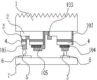
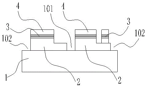
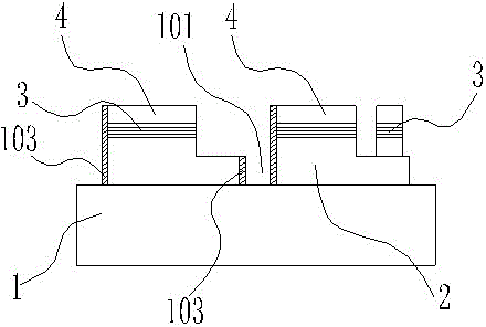
[0033] Such as figure 1 As shown, a high-voltage flip-chip LED chip manufacturing method includes a substrate 7 and a sapphire substrate 1, and the lower surface of the sapphire substrate (1) is sequentially provided with an n-type GaN layer 2, a quantum well active region 3, p type GaN layer 4, wherein, on the sapphire substrate 1, a chip interconnection region 101 and a scribe region 102 are provided; the walls of the chip interconnection region 1...


PUM

PropertyMeasurementUnit
Thicknessaaaaaaaaaa
Etching depthaaaaaaaaaa

Abstract

The invention discloses a high-voltage and inverted LED (light emitting diode) chip and a manufacturing method thereof. A chip interconnection region (101) and a cutting channel region (102) are arranged on a sapphire substrate (1); SiO2 films are arranged on a wall of the chip interconnection region (101) and a wall of the cutting channel region (102); a current diffusion layer (104) is arranged on the lower surface of a p type GaN layer (4); metal electrodes (105) are arranged on the lower surface of the chip interconnection region (101) and the lower surface of the current diffusion layer (104); and two pieces of cathode metals (6) are arranged on the upper surface of the substrate (7) and are connected with the metal electrodes (105) through solder paste (5). Advantages of a high-voltage chip and advantages of an inverted chip are combined to form the high-voltage and inverted chip. The chip can be packaged by an inverted chip packaging technology, has the advantages of high lighting effect of the high-voltage chip and low power source combination cost, and has a wide application prospect.

Description

technical field [0001] The invention relates to the field of manufacturing optoelectronic light-emitting devices, in particular to a high-voltage flip-chip LED chip and a manufacturing method thereof. Background technique [0002] Semiconductor lighting is an emerging technology, which has outstanding advantages such as environmental protection, energy saving and safety, and is the star of hope for the new generation of lighting. Light-emitting diode (LED) is a light-emitting device that converts electrical energy into light energy. As a result, LEDs have been used more and more widely due to their outstanding energy-saving and environmental protection features, and have been expanded to high-end applications including automotive headlights and LCD backlights. Recently, they have begun to enter the general lighting market. [0003] With the application of LEDs in the field of lighting more and more widely, the traditional low-voltage front-mount LED chips cannot work under ...

Claims


Application Information

Patent Timeline
IPC IPC(8): H01L33/44H01L33/62H01L33/00
CPCH01L33/44H01L33/007H01L33/62
Inventor 武乐可
Owner 江苏汉莱科技有限公司
Features
  • R&D
  • Intellectual Property
  • Life Sciences
  • Materials
  • Tech Scout
  • Unparalleled Data Quality
  • Higher Quality Content
  • 60% Fewer Hallucinations
Learn More