Adhesive film, laminate and cured product thereof, semiconductor device and method for producing same

An adhesive film and compound technology, which is applied in the fields of semiconductor/solid-state device manufacturing, semiconductor devices, and semiconductor/solid-state device components, etc., can solve problems such as difficult filling, and achieve the effect of improving reliability and improving yield.

Active Publication Date: 2019-01-22
SUMITOMO BAKELITE CO LTD
View PDF7 Cites 0 Cited by
  • Summary
  • Abstract
  • Description
  • Claims
  • Application Information

AI Technical Summary

Problems solved by technology

However, as semiconductor devices become thinner and miniaturized, the soldering portion becomes narrower in pitch / gap, so even if a liquid sealing resin (underfill material) is supplied after soldering, the liquid sealing resin (underfill material) will not Will not spread over the gaps, causing problems that are difficult to fill completely

Method used


Image

  • Adhesive film, laminate and cured product thereof, semiconductor device and method for producing same
  • Adhesive film, laminate and cured product thereof, semiconductor device and method for producing same
  • Adhesive film, laminate and cured product thereof, semiconductor device and method for producing same

Examples


Embodiment 1

[0261]

[0262] 14.26 parts by weight of cresol novolak resin (manufactured by DIC Corporation, KA-1160), 39.73 parts by weight of bisphenol F-type epoxy resin (manufactured by DIC Corporation, EXA-830LVP), trimellitic acid ( 10.50 parts by weight of Tokyo Chemical Industry Co., Ltd., 5.07 parts by weight of phenoxy resin (manufactured by Mitsubishi Chemical Corporation, YX-6954) as a film-forming resin, 2-phenyl-4-methylimidazole as a curing accelerator (Shikoku Chemical Industry Co., Ltd., 2P4MZ) 0.09 parts by weight, 3-glycidoxypropyltrimethoxysilane (Shikoku Chemical Industry Co., Ltd., KBM-403) 0.35 parts by weight as a silane coupling agent, and two 30.00 parts by weight of a silica filler (manufactured by Admatechs, SC1050, average particle diameter: 0.25 μm) was dissolved and dispersed in methyl ethyl ketone to prepare a resin varnish having a resin concentration of 50%.

[0263] The obtained adhesive film varnish was coated on a substrate polyester film (base film, ...

Embodiment 2

[0265]

[0266] 25.15 parts by weight of biphenyl aralkyl type phenolic resin (Meiwa Kasei Co., Ltd., MEH-7851), 32.10 parts by weight of bisphenol F type epoxy resin (manufactured by DIC Corporation, EXA-830LVP), and a compound having flux activity 8.60 parts by weight of trimellitic acid (manufactured by Tokyo Chemical Industry Co., Ltd.), 3.90 parts by weight of phenoxy resin (manufactured by Mitsubishi Chemical Corporation, YX-6954) as a film-forming resin, 2-phenyl- 0.05 parts by weight of 4-methylimidazole (manufactured by Shikoku Chemical Industry Co., Ltd., 2P4MZ), 3-glycidoxypropyltrimethoxysilane (manufactured by Shin-Etsu Chemical Co., Ltd., KBM-403) as a silane coupling agent 0.20 parts by weight, 5.00 parts by weight of silica filler (manufactured by Japan Aerosil Co., Ltd., AEROSIL 200) and 25.00 parts by weight of silica filler (manufactured by Admatechs, YA050C with an average particle diameter of 0.05 μm) were dissolved and dispersed in methyl ethyl ketone ,...

Embodiment 3

[0269]

[0270] 10.20 parts by weight of phenol aralkyl resin (XLC-4L manufactured by Mitsui Chemicals Co., Ltd.), 22.00 parts by weight of bisphenol A type epoxy resin (manufactured by DIC Corporation, EPICLON 840-S), and phenolphthalein ( Tokyo Chemical Industry Co., Ltd.) 8.20 parts by weight, 9.30 parts by weight of an epoxy-group-containing acrylate copolymer (manufactured by NagaseChemteX Corporation, SG-P3) as a film-forming resin, 2-methylimidazole ( Shikoku Chemical Industry Co., Ltd., 2MZ-H) 0.05 parts by weight, 3-methacryloxypropyltriethoxysilane (Shikoku Chemical Industry Co., Ltd., KBE-503) as a silane coupling agent 0.25 parts by weight A resin varnish having a resin concentration of 50% was prepared by dissolving and dispersing 50.00 parts by weight of a silica filler (manufactured by Admatechs, SC1050 with an average particle diameter of 0.25 μm) in methyl ethyl ketone.

[0271] The obtained adhesive film varnish was coated on a substrate polyester film (bas...


PUM

PropertyMeasurementUnit
surface roughnessaaaaaaaaaa
particle sizeaaaaaaaaaa
widthaaaaaaaaaa

Abstract

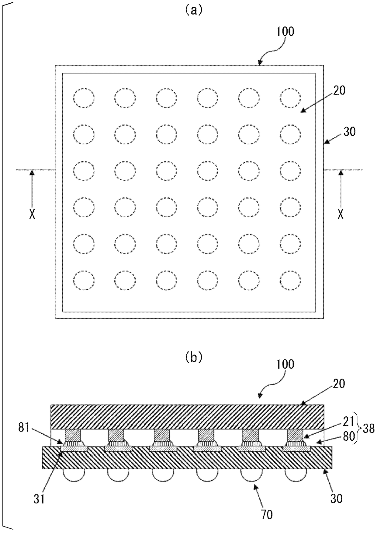
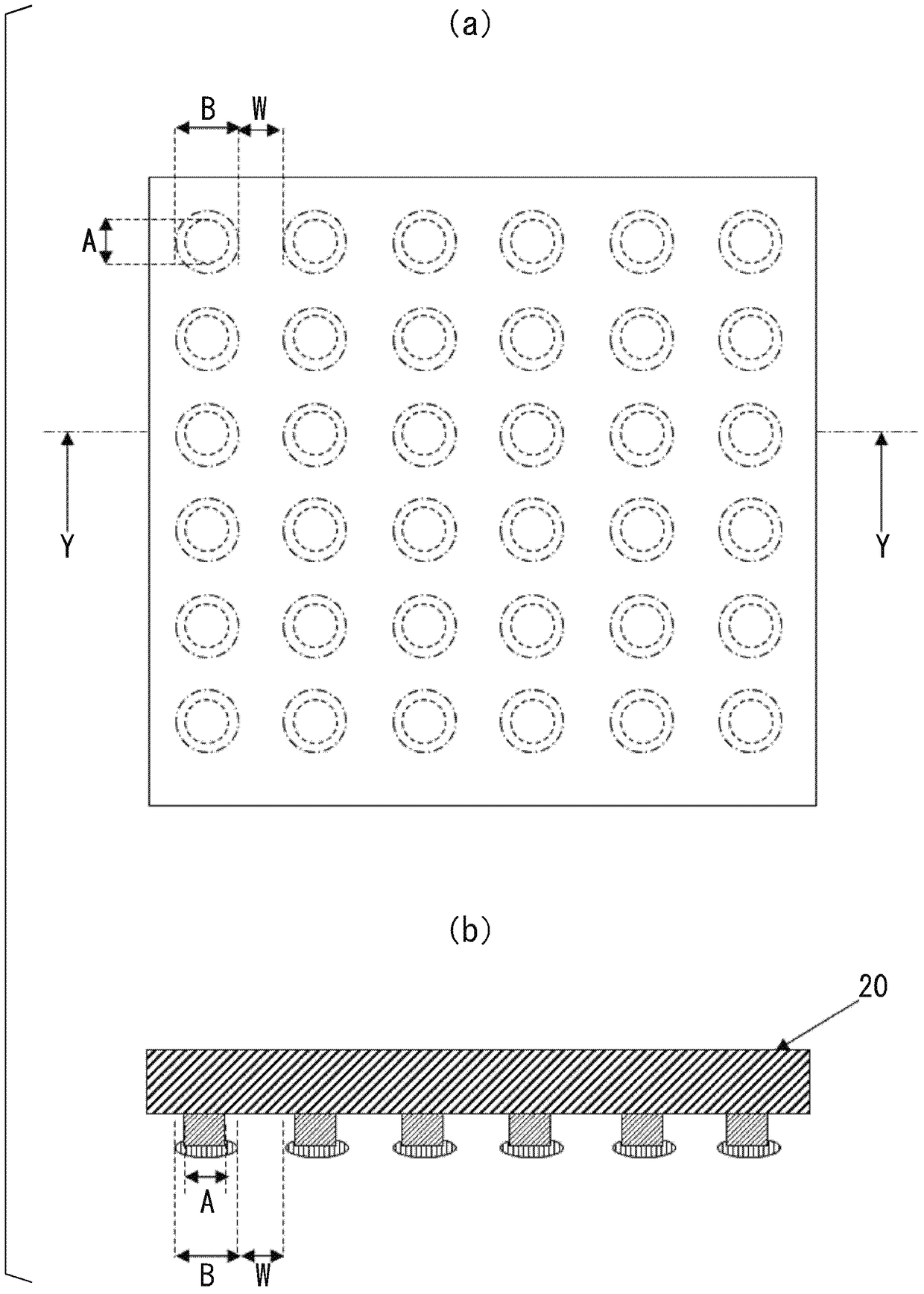
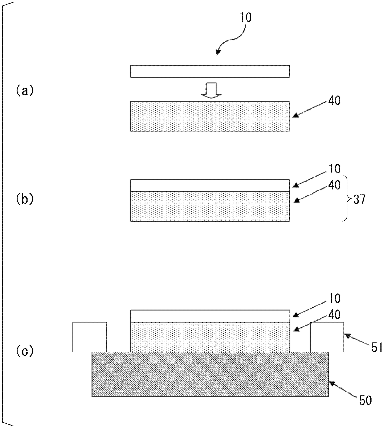
An object of the present invention is to provide an adhesive film (10) having both sufficient transparency and reliability of welded portions. The present invention is an adhesive film (10) for connection between terminals, which is interposed between an electronic component (20) having a plurality of first terminals (21) on its surface and a plurality of second terminals corresponding to the above-mentioned terminals (21) (31) Between the circuit components (30), the above-mentioned first terminal and the second terminal are electrically connected, the width of the above-mentioned first terminal (21) is not less than 3 μm and not more than 100 μm, and the above-mentioned first terminal (21) has a surface covering the terminal At least a part of the metal composition with a low melting point satisfies 0.6<A / B<1.4 when the width of the first terminal (21) is A and the width of the metal composition is B, and B satisfies 2 μm or more and 170 μm Hereinafter, the distance between the metal compositions of adjacent first terminals (21) is not less than 3 μm and not more than 60 μm, and the adhesive film (10) is made of a resin containing a filler material in an amount of not less than 10% by weight and not more than 70% by weight. The composition composition has a surface roughness Ra of 0.03 μm or more and 1.0 μm or less.

Description

technical field [0001] The present invention relates to an adhesive film, an adhesive film integrated with a dicing sheet, an adhesive film integrated with a back grinding tape, an adhesive film integrated with a back grinding tape and a dicing sheet, and a laminate , a cured product of a laminate, a semiconductor device, and a method for manufacturing the semiconductor device. [0002] This application claims priority based on Japanese Patent Application No. 2013-045020 for which it applied in Japan on March 7, 2013, and uses the content here. Background technique [0003] In recent years, with the demand for higher functionality and thinner and shorter electronic equipment, the number of semiconductor devices used in these electronic equipment has also increased compared to the past, and miniaturization and multi-pins have gradually progressed. Soldering is widely used in order to obtain electrical connections between electronic components in these semiconductor devices, ...

Claims


Application Information

Patent Timeline
Patent Type & Authority Patents(China)
IPC IPC(8): H01L21/60H01L21/683C09J163/00C09J11/04C09J7/35C08G59/62
CPCC09J11/04C09J163/00H01L2224/13005H01L24/13H01L24/16H01L24/29H01L24/32H01L21/6836H01L24/81H01L24/83H01L24/91H01L2221/68377H01L2224/13017H01L2224/13082H01L2224/16058H01L2224/27436H01L2224/2929H01L2224/29298H01L2224/73104H01L2224/73204H01L2224/81191H01L2224/83191H01L2224/13076H01L2224/16237H01L23/293H01L23/295H01L21/563H01L2224/26175H01L2224/8385H01L2224/9211H01L2224/81903C08G59/621C09J2203/326C09J7/35H01L2924/207H01L2224/81H01L2224/83
Inventor 前岛研三
Owner SUMITOMO BAKELITE CO LTD
Why Eureka
Try Eureka