Shifting register, drive method thereof, drive circuit and display device

A shift register, voltage terminal technology, applied in static memory, digital memory information, instruments, etc., can solve the problems of large number of uses, large occupied area of ​​thin film transistors, inability to meet narrow borders and low power consumption, etc., to reduce the number of uses , the effect of simple structure and low power consumption

Active Publication Date: 2015-11-11
BOE TECH GRP CO LTD +1
View PDF4 Cites 41 Cited by
  • Summary
  • Abstract
  • Description
  • Claims
  • Application Information

AI Technical Summary

Problems solved by technology

[0003] In order to solve the above problems, the present invention provides a shift register and its driving method, driving circuit and display device, which are used to solve the problem that the number of thin film transistors used in the row driving circuit of the array substrate in the prior art is large, resulting in the occupation of the thin film transistors. Large area, unable to meet the requirements of narrow border and low power consumption

Method used


Image

  • Shifting register, drive method thereof, drive circuit and display device
  • Shifting register, drive method thereof, drive circuit and display device
  • Shifting register, drive method thereof, drive circuit and display device

Examples


Embodiment 1

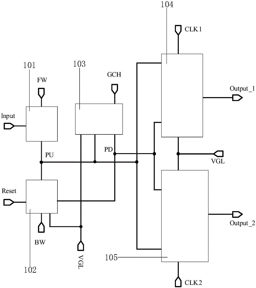
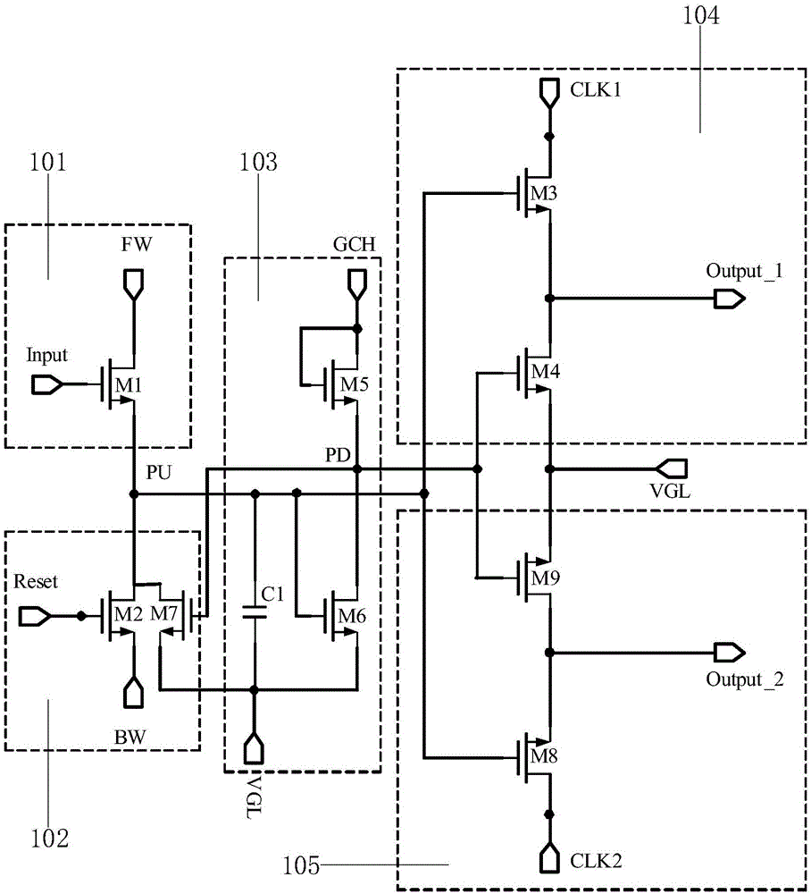
[0053] figure 1It is a schematic structural diagram of a shift register provided by Embodiment 1 of the present invention. Such as figure 1 As shown, the shift register includes an input unit 101, a reset unit 102, a control unit 103, a first output unit 104 and a second output unit 105, and the first output unit 104 is used to connect the first node PU and the second Under the potential control of the node PD, the output signal of the first output terminal Output_1 is controlled according to the input signal of the fifth voltage terminal VGL and the first clock signal terminal CLK1, and the second output unit 105 is used for connecting the first node PU and the second node Under the potential control of the PD, the output signal of the second output terminal Output_2 is controlled according to the input signal of the fifth voltage terminal VGL and the second clock signal terminal CLK2 . The shift register provided by this embodiment shares the first node PU and the second n...

Embodiment 2

[0061] This embodiment provides a method for driving a shift register. The shift register includes the shift register provided in Embodiment 1. For details, please refer to the description in Embodiment 1, which will not be repeated here. The first voltage terminal FW provided by this embodiment is at high level, the second voltage terminal BW is at low level, the third voltage terminal VGL is at low level, the fourth voltage terminal GCH is at high level, and the fifth voltage terminal VGL is low level. At this time, the shift register is in a forward scanning state.

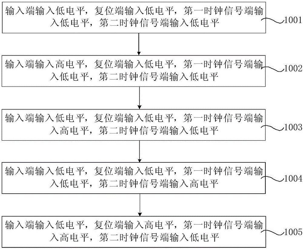
[0062] image 3 It is a flow chart of a driving method for a shift register provided in Embodiment 2 of the present invention, Figure 4 A working sequence diagram of a shift register provided by Embodiment 2 of the present invention. Such as image 3 and Figure 4 As shown, the driving method includes:

[0063] Step 1001: input a low level at the input terminal, input a low level at the reset terminal, i...

Embodiment 3

[0075]This embodiment provides a method for driving a shift register. The shift register includes the shift register provided in Embodiment 1. For details, please refer to the description in Embodiment 1, which will not be repeated here. The first voltage terminal FW provided by this embodiment is at low level, the second voltage terminal BW is at high level, the third voltage terminal VGL is at low level, the fourth voltage terminal GCH is at high level, and the fifth voltage terminal VGL is low level. At this time, the shift register is in a reverse scanning state.

[0076] Figure 5 It is a flow chart of a driving method for a shift register provided in Embodiment 3 of the present invention, Figure 6 A working sequence diagram of a shift register provided by Embodiment 3 of the present invention. Such as Figure 5 and Figure 6 As shown, the driving method includes:

[0077] Step 2001: input a low level at the input terminal, input a low level at the reset terminal, ...


PUM


Abstract

The invention discloses a shifting register, a drive method thereof, a drive circuit and a display device. The shifting register comprises an input unit, a reset unit, a control unit, a first output unit and a second output unit. The first output unit is used for controlling an output signal output by a first output end according to input signals of a fifth voltage end and a first clock signal end under the potential control of a first node and a second node. The second output unit is used for controlling an output signal of a second output end according to input signals of the fifth voltage end and a second clock signal end under the potential control of the first node and the second node. According to the shifting register, on the premise of not increasing control signals and ensuring functions of the shifting register, every two lines share the first node and the second node, and therefore the number of thin film transistors which are used is decreased, the occupied area of the thin film transistors is reduced, the structure of the shifting register can be simple, and the requirements for narrow frames and low power consumption are met.

Description

technical field [0001] The invention relates to the field of display technology, in particular to a shift register, a driving method thereof, a driving circuit and a display device. Background technique [0002] In the existing array substrate row drive circuit (GateDriveronArray, GOA), each row of shift registers requires a pull-up node and a pull-down node, so that the number of thin film transistors is increased, and the occupied area of ​​the thin film transistor is large, resulting in a large area of ​​the array substrate. The structure of the row driving circuit is complex, which cannot meet the requirements of narrow frame and low power consumption. Contents of the invention [0003] In order to solve the above problems, the present invention provides a shift register and its driving method, driving circuit and display device, which are used to solve the problem that the number of thin film transistors used in the row driving circuit of the array substrate in the pr...

Claims


Application Information

Patent Timeline
Patent Type & Authority Applications(China)
IPC IPC(8): G11C19/28G09G3/20
Inventor 冯思林李红敏
Owner BOE TECH GRP CO LTD
Why Eureka
Try Eureka