Check patentability & draft patents in minutes with Patsnap Eureka AI!

Alignment mark for silicon carbide device and preparation method of alignment mark

An alignment mark, silicon carbide technology, applied in semiconductor/solid-state device manufacturing, semiconductor devices, electrical solid-state devices, etc., can solve the problems of increased cost, increased difficulty, and long alignment mark manufacturing time, so as to reduce misoperation , the effect of reducing the rework rate

Inactive Publication Date: 2015-11-11
GLOBAL POWER TECH CO LTD
View PDF4 Cites 5 Cited by
  • Summary
  • Abstract
  • Description
  • Claims
  • Application Information

AI Technical Summary

Problems solved by technology

[0008] First, the silicon carbide material itself is translucent, and the contrast between the alignment mark formed on the wafer and the background is not enough. It is difficult to identify and locate through the artificial naked eye and image recognition equipment, which easily leads to misoperation and high rework rate.
Even increasing the depth of the groove as the alignment mark, or increasing the height of the protrusion as the alignment mark cannot completely solve the problem
[0009] Second, the hardness of the silicon carbide material is relatively high, and it is difficult to etch. It takes a long time to etch the groove or protrusion as the alignment mark, and the thickness of the photoresist used as the etching mask is also relatively large, which makes the The manufacturing time of the quasi-mark is very long, the difficulty becomes greater, and the cost increases
However, due to the need for some unique long-term high-temperature processing steps during the preparation of silicon carbide devices, no metal or other non-silicon carbide substances can be left on the wafer surface during this high-temperature processing step.
Therefore, the metal layer needs to be removed after the alignment marks are formed on the wafer, which complicates the manufacturing process of silicon carbide devices and increases the possibility of contamination of the wafer or equipment

Method used


Image

  • Alignment mark for silicon carbide device and preparation method of alignment mark
  • Alignment mark for silicon carbide device and preparation method of alignment mark
  • Alignment mark for silicon carbide device and preparation method of alignment mark

Examples


Embodiment 1

[0035] The method for preparing an alignment mark for a silicon carbide device provided in this embodiment includes the following steps:

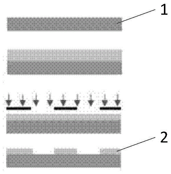
[0036] S1: Form a patterned mask 2 on the surface of the silicon carbide substrate 1, such as image 3 shown;

[0037] S2: With the help of the above-mentioned patterned mask 2, perform dry etching on the area of ​​the surface of the above-mentioned silicon carbide substrate 1 except for the alignment mark area 3 to form a micro-mask area 4, so that the alignment mark area 3 and the micro-mask The brightness of the mold area 4 contrasts and thus forms an alignment mark, such as Figure 4 shown.

[0038] like Figure 5 As shown, compared with the alignment mark region 3, the surface of the micro-mask region 4 is very rough. When the micro-mask area 4 is viewed from a low-magnification microscope, the surface of the micro-mask area 4 presents black spots connected in sheets, such as Image 6 shown.

[0039] In a preferred implementation...

Embodiment 2

[0042] This embodiment provides an alignment mark for a silicon carbide device. An alignment mark region 3 is formed on the surface of a silicon carbide substrate 1 . The brightness of the alignment mark region 3 and the micro-mask region 4 form a contrast.

[0043] The aforementioned micro-mask region 4 is a region formed by performing dry etching on the surface of the silicon carbide substrate 1 except for the alignment mark region 3 .


PUM


Abstract

The invention discloses an alignment mark for a silicon carbide device and a preparation method of the alignment mark. The preparation method comprises the following steps: forming a patterned mask on the surface of a silicon carbide substrate; carrying out dry etching on the region, except for an alignment mark region, on the surface of the silicon carbide substrate by virtue of the patterned mask, so as to form a micro-mask region; and forming a contrast by the brightness of the alignment mark region and the brightness of the micro-mask region, thereby forming the alignment mark. According to the preparation method, the micro-mask region is formed in the region, except for the alignment mark region, on the surface of the silicon carbide substrate by dry etching; the contrast is formed by the brightness of the alignment mark region and the brightness of the micro-mask region, thereby forming the alignment mark; and recognition and localization can be realized through human eyes and image recognition equipment, so that a misoperation can be reduced; and the rework rate is reduced. In addition, the brightness contrast between the alignment mark region and the micro-mask region is formed by the roughness of the silicon carbide substrate material; and a novel material is not introduced, so that no pollution is introduced.

Description

technical field [0001] The invention relates to the field of semiconductor processing technology for silicon carbide devices. More specifically, it relates to an alignment mark for a silicon carbide device and a preparation method thereof. Background technique [0002] As a third-generation broadband compound semiconductor material, silicon carbide has incomparable advantages over traditional silicon and gallium arsenide materials in terms of band gap, maximum field strength, doping concentration, and thermal conductivity, and is especially suitable for high-voltage, High-frequency, high-power, high-irradiation and photoelectric detection fields of certain wavelengths. At present, silicon carbide has attracted the attention of researchers in power microwave and optoelectronic devices. [0003] Compared with traditional silicon-based devices, silicon carbide devices have the advantages of simple structure, small size and high performance based on the advantages of silicon c...

Claims


Application Information

Patent Timeline
IPC IPC(8): H01L21/02H01L23/544
CPCH01L21/02H01L23/544H01L2223/54426
Inventor 何钧仇坤苗青张瑜洁牛喜平
Owner GLOBAL POWER TECH CO LTD
Features
  • R&D
  • Intellectual Property
  • Life Sciences
  • Materials
  • Tech Scout
  • Unparalleled Data Quality
  • Higher Quality Content
  • 60% Fewer Hallucinations
Learn More