Terahertz filter and manufacturing method thereof
A manufacturing method and filter technology, which can be applied to waveguide-type devices, electrical components, circuits, etc., can solve the problems of narrow filtering range of filters, adding terahertz filters, and poor scalability.
- Summary
- Abstract
- Description
- Claims
- Application Information
AI Technical Summary
Problems solved by technology
Method used
Image
Examples
Embodiment 1
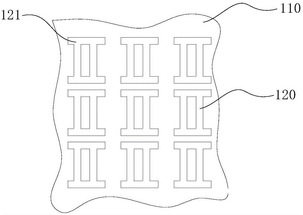
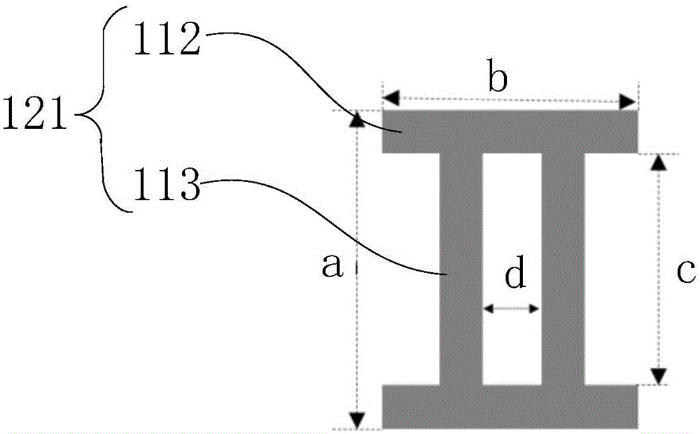
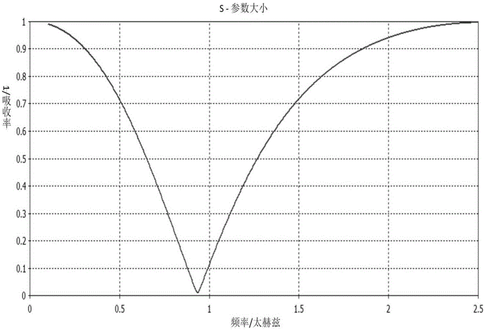
[0046] This embodiment provides a terahertz filter, and its specific implementation structure is as follows figure 1 , figure 2 , image 3 , Figure 4 shown, may include;
[0047] The polymer material layer 110 and the metal layer 120, wherein the polymer material layer is made of a flexible polymer material, for example, Parylene (parylene), PMMA (Polymethylmethacrylate, polymethyl methacrylate), PDMS (polydimethylsiloxane, polydimethylsiloxane) Silicone) and other polymer materials with excellent flexibility and light transmission, such as figure 2As shown, the metal layer 120 is a sheet structure 121 including horizontal bars 122 and vertical bars 123; the metal layer can be made of copper, aluminum, silver and other metal materials with low resistivity and good conductivity; the sheet structure is periodically distributed in within the polymeric material layer 110 .
[0048] In the specific implementation process of the embodiment of the present invention, in order ...
Embodiment 2
[0058] This embodiment provides a manufacturing process of the terahertz filter as in Embodiment 1 such as Figure 7 As shown, the following processing steps are included:
[0059] Step S701, prepare the sheet, use the double-thrown silicon wafer as the supporting substrate sheet 1 of flexible structure, grow a layer of silicon dioxide on the surface of the substrate as the insulating medium layer 2 by thermal oxidation, the thickness of this layer of silicon dioxide can be 300nm;
[0060] Step S702, deposit a polymer on the surface of the silicon wafer, the polymer is a flexible polymer material (such as Parylene, PMMA, PDMS and other polymer materials with excellent flexibility and light transmittance), with a thickness of 5 μm to 200 μm, forming the first layer polymeric material 111;
[0061] Step S703, the first layer of polymer material is used as the first substrate of the filter, after conventional cleaning, the photoresist 3 is applied, and the mask of the sheet str...
PUM
| Property | Measurement | Unit |
|---|---|---|
| thickness | aaaaa | aaaaa |
| thickness | aaaaa | aaaaa |
| length | aaaaa | aaaaa |
Abstract
Description
Claims
Application Information


