High-precision printed circuit board

A printed circuit board, high-precision technology, applied in the direction of printed circuits, printed circuit components, circuit heating devices, etc., can solve the problems that cannot be realized, the automatic detection system is expensive, and cannot be inspected

Inactive Publication Date: 2015-11-11
ZHENJIANG HUAYIN PRINTED CIRCUIT BOARD
View PDF3 Cites 2 Cited by
  • Summary
  • Abstract
  • Description
  • Claims
  • Application Information

AI Technical Summary

Problems solved by technology

Because the automatic detection system of printed circuit boards in foreign countries is too expensive, and the automatic detection equipment of printed circuit boards in the true sense has not been developed in China, most domestic circuit board manufacturers still use manual inspection with a magnifying glass or a projector. check side
Due to the high labor intensity of manual inspection, the eyes are prone to fatigue, and the missed inspection rate is high
Moreover, with the development of electronic products towards miniaturization and digitalization, printed circuit boards are also developing towards high density and high precision.
For higher density and precision circuit boards (0.12×0.10mm), it is completely impossible to inspect
Due to the backwardness of detection methods, the current domestic multi-layer board (8-12 layer) product pass rate is only 50, 60%
[0004] Due to its high precision, high-precision printed circuit boards have many connected and installed electronic components and wiring, so they must have high heat dissipation to ensure the normal operation of the circuit board when it is put into work. The circuit board cannot fully meet this demand and needs to be improved urgently

Method used


Image

  • High-precision printed circuit board
  • High-precision printed circuit board

Examples


Embodiment Construction

[0014] The present invention will be further described below in conjunction with the accompanying drawings.

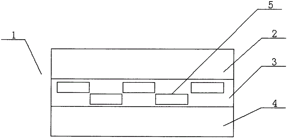
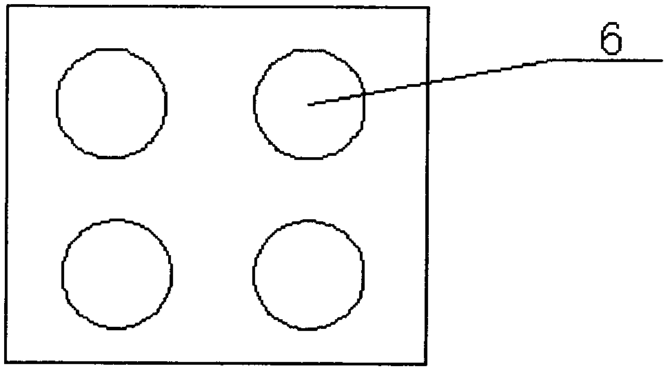
[0015] see figure 1 and figure 2 As shown, the technical solution adopted in this specific embodiment is: it includes a circuit board body 1; the circuit board body 1 is composed of a circuit layer 2, an insulating layer 3 and a heat conducting layer 4, and an insulating layer is provided at the bottom of the circuit layer 2 3. A thermal conduction layer 4 is provided on the lower part of the insulating layer 3; several heat sinks 5 are provided inside the insulating layer 3, and through holes 6 for placing electronic component pins are provided on the heat sink 5.

[0016] The two adjacent heat sinks 5 are set up and down alternately, which increases the heat dissipation area, makes the temperature in the insulating layer more uniform, and is beneficial to the overall heat dissipation.

[0017] The working principle of this specific embodiment: by adding a heat sin...


PUM


Abstract

A high-precision printed circuit board is disclosed. The invention relates to the circuit board technology field. The printed circuit board comprises a circuit board body. The circuit board body is formed by a circuit layer, an insulating layer and a heat conduction layer. A lower portion of the circuit layer is provided with the insulating layer. A lower portion of the insulating layer is provided with the heat conduction layer. An internal portion of the insulating layer is provided with several cooling fins. The cooling fins are provided with through holes used for placing electronic component pins. The printed circuit board possesses high precision and simultaneously has a good heat dissipation function. Faults brought by heating after the circuit board is operated are reduced and applicability is high.

Description

technical field [0001] The invention relates to the technical field of circuit boards, in particular to high-precision printed circuit boards. Background technique [0002] The names of circuit boards are: circuit board, PCB board, aluminum substrate, high frequency board, thick copper board, impedance board, PCB, ultra-thin circuit board, ultra-thin circuit board, printed (copper etching technology) circuit board, etc. The circuit board makes the circuit miniaturized and intuitive, and plays an important role in mass production of fixed circuits and optimizing the layout of electrical appliances. The circuit board can be called a printed circuit board or a printed circuit board, and the English name is (Printed Circuit Board) PCB. Printed circuit boards are the providers of electrical connections for electronic components. Its development has a history of more than 100 years; its design is mainly layout design; the main advantage of using circuit boards is that it greatly...

Claims


Application Information

Patent Timeline
Patent Type & Authority Applications(China)
IPC IPC(8): H05K1/02
CPCH05K1/0209H05K1/021H05K2201/06
Inventor 赵晶凯
Owner ZHENJIANG HUAYIN PRINTED CIRCUIT BOARD
Why Eureka
Try Eureka