Digital phase shift point diffraction interferometer and optical system wave aberration measuring method

A point diffraction interferometer and digital phase shift technology, applied in the field of optical detection, can solve the problems of large pinhole window distance and poor interference fringe ratio, and achieve adjustable contrast ratio, accurate phase shift, and adjustable interference fringe density. Effect

Active Publication Date: 2015-11-25
SHANGHAI INST OF OPTICS & FINE MECHANICS CHINESE ACAD OF SCI
View PDF1 Cites 7 Cited by
  • Summary
  • Abstract
  • Description
  • Claims
  • Application Information

AI Technical Summary

Problems solved by technology

[0003] The purpose of the present invention is to overcome the deficiencies of the above-mentioned prior art, and to provide a digital phase-shift point diffraction interferometer and a method for measuring wave aberration of an optical system. Modulator, the spatial light modulator in front of the optical system is set as a grating through the computer, digital phase shift can be achieved by digitally moving the grating in the direction perpendicular to the grating lines, and the spatial light modulator of the image plane is set as a pinhole window mask , through the combined use of two spatial light modulators, the distance between the pinhole and the window of the image plane mask can be adjusted, the grating period is small, the distance between the pinhole window is large, and the grating period is large, the pinhole The distance between the windows is small, so as to avoid the problem of poor contrast of interference fringes, and also make the density of interference fringes adjustable

Method used


Image

  • Digital phase shift point diffraction interferometer and optical system wave aberration measuring method
  • Digital phase shift point diffraction interferometer and optical system wave aberration measuring method
  • Digital phase shift point diffraction interferometer and optical system wave aberration measuring method

Examples


Embodiment Construction

[0028] The present invention will be further described below in conjunction with the embodiments and accompanying drawings, but the protection scope of the present invention should not be limited thereby.

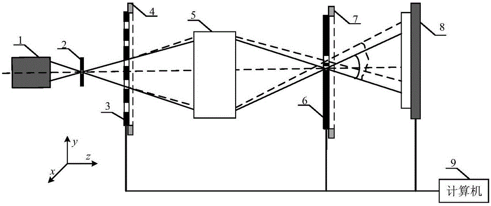
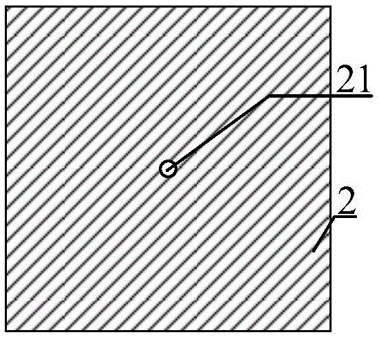
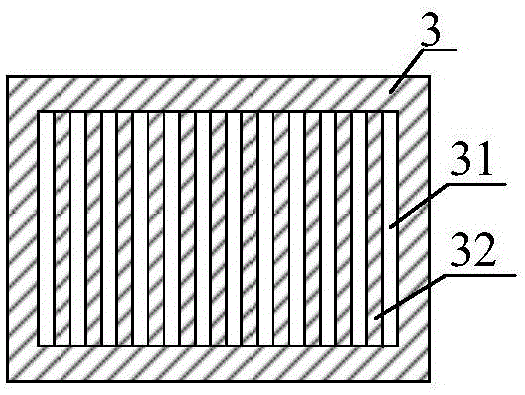
[0029] see first figure 1 , figure 1 It is the optical path structure diagram of the digital phase shift point diffraction interferometer of the present invention, by figure 1 It can be seen that the digital phase-shifting point diffraction interferometer of the present invention is characterized in that the interferometer includes a light source 1, and along the output beam direction of the light source 1 are a small hole mask 2, a first spatial light modulator 3, and a second spatial light modulator. device 6 and a two-dimensional photodetector 8, the output end of the two-dimensional photodetector 8 is connected to the input end of the computer 9; the first spatial light modulator 3 and the second spatial light modulator 6 are placed in the first spatial light modulator...


PUM


Abstract

The invention relates to a digital phase shift point diffraction interferometer and an optical system wave aberration measuring method. The interferometer comprises a light source, a small-hole mask, a first spatial light modulator, a second spatial light modulator, a two dimension photoelectric detector and a computer, wherein the first spatial light modulator is set as a raster through the computer, and is used as a splitter; the second spatial light modulator is set as a pin hole window mask, and is used as a filter for filtering diffraction orders except 0 order and +1 (or -1) order to enable the 0-order light to realize diffraction production through the pin hole to generate a quasi-ideal spherical wave so as to use the quasi-ideal spherical wave as the reference light wave; the +1 (or -1) order light is used as the object light wave through the window; then interference occurs between the reference light wave and the object light wave so that an interferogram is obtained; and the optical system wave aberration to be measured can be extracted from the interferogram. For the digital phase shift point diffraction interferometer, the distance among image plane convergent points for the object light wave and the reference light wave is adjustable, and great interference fringe density can be realized without reducing the interference fringe contrast.

Description

technical field [0001] The invention belongs to the field of optical detection, and in particular relates to a digital phase shift point diffraction interferometer and a method for measuring wave aberration of an optical system. Background technique [0002] The wave aberration measurement of optical imaging system is very important for imaging quality control. Interferometry is an important method for measuring wave aberration in optical imaging systems. Traditional interferometry uses a spherical reference mirror as a reference surface to generate spherical waves as reference light waves, which interfere with the object light waves to be measured to form interference fringes. The measurement accuracy of this type of method is limited by the surface shape accuracy of the reference surface. Due to the limitation of the manufacturing technology and cost of the high-precision reference surface shape, this type of method cannot meet the high-precision wave aberration measuremen...

Claims


Application Information

Patent Timeline
Patent Type & Authority Applications(China)
IPC IPC(8): G01J9/02G01M11/02
CPCG01J9/02G01M11/02
Inventor 戴凤钊王向朝唐锋
Owner SHANGHAI INST OF OPTICS & FINE MECHANICS CHINESE ACAD OF SCI
Why Eureka
Try Eureka