Wafer Processing Method

A processing method and wafer technology, which is applied in the manufacture of electrical components, circuits, semiconductors/solid-state devices, etc., can solve the problems of complex process, unfavorable reduction of process time, and reduction of process cost, so as to achieve process simplification, save process cost, and save The effect of process time

Active Publication Date: 2019-03-12
SEMICON MFG INT (SHANGHAI) CORP
View PDF6 Cites 0 Cited by
  • Summary
  • Abstract
  • Description
  • Claims
  • Application Information

AI Technical Summary

Problems solved by technology

[0006] However, the existing process for forming TSV structures is complicated, which is not conducive to reducing process time and process cost

Method used


Image

  • Wafer Processing Method
  • Wafer Processing Method
  • Wafer Processing Method

Examples


Embodiment Construction

[0032] As mentioned in the background art, the existing process for forming the through-silicon via structure is complicated, which is not conducive to reducing process time and process cost.

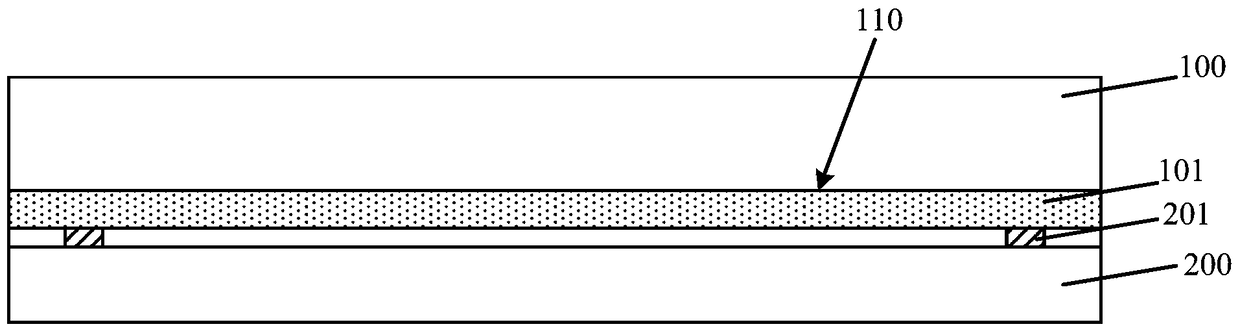
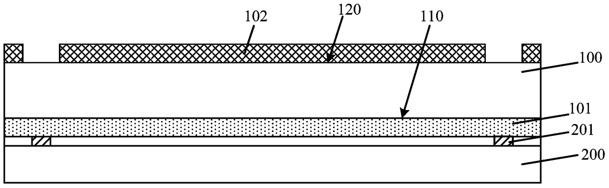
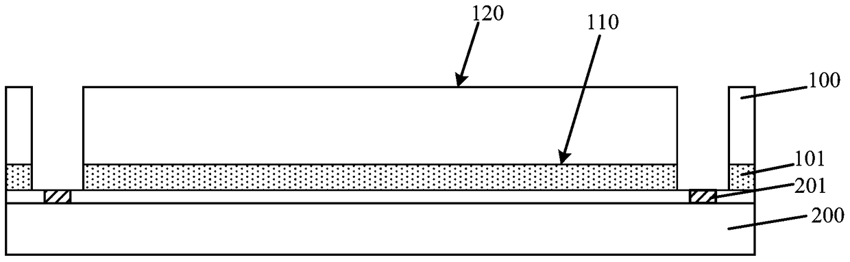
[0033] After research, it is found that after thinning the semiconductor substrate, an etching process needs to be used to etch from the second surface of the semiconductor substrate, so as to form through holes in the semiconductor substrate and the device layer. However, the process of forming the through hole is complicated. like Figure 1 to Figure 4 Shown is a schematic cross-sectional structure diagram of the process of forming a through hole in a semiconductor substrate and a device layer.

[0034] Please refer to figure 1 , provide a semiconductor substrate 100 and a carrier base 200, the first surface 110 of the semiconductor substrate 100 has a device layer 101, the first surface 110 of the semiconductor substrate 100 is bonded to the carrier base 200 through the device laye...


PUM

PropertyMeasurementUnit
thicknessaaaaaaaaaa

Abstract

The invention provides a wafer processing method. A first surface of a bearing substrate is provided with a positioning mark. A substrate to be processed has a first surface and a second surface opposed to the first surface. The substrate to be processed has a device zone and an edge zone surrounding the device zone. The method comprises the following steps of bonding the first surface of the bearing substrate and the first surface of the substrate to be processed, wherein, the positioning mark is located in the edge zone of the substrate to be processed; applying trimming technologies on the substrate to be processed to make the radius of the substrate to be processed smaller and completely expose the positioning mark on the first surface of the bearing substrate; forming a mask layer on the second surface of the substrate to be processed through positioning of the positioning mark, wherein an opening exposing a part of the second surface of the substrate to be processed is arranged inside the mask layer; etching the substrate to be processed on the bottom of the opening with the mask layer as a mask until the first surface of the bearing substrate is exposed; and forming a through hole in the substrate to be processed. By means of the wafer processing method, silicon through hole forming technologies are simplified.

Description

technical field [0001] The invention relates to the technical field of semiconductor manufacturing, in particular to a wafer processing method. Background technique [0002] In the semiconductor manufacturing process, a wafer (Wafer) on which semiconductor devices have been formed on the surface can be cut into multiple chips, and then each chip is packaged to form a required integrated circuit or chip device. Taking Wafer Level Chip Size Packaging (WLCSP) technology as an example, the wafer is packaged and tested and then cut to obtain a single finished chip. The size of the packaged chip is exactly the same as that of the bare chip. The size of the chip packaged by the wafer-level chip size packaging technology can be highly miniaturized, and the cost of the chip is significantly reduced with the reduction of the chip size and the increase of the wafer size. [0003] With the continuous development of semiconductor manufacturing technology, the feature size of semiconduct...

Claims


Application Information

Patent Timeline
Patent Type & Authority Patents(China)
IPC IPC(8): H01L21/02H01L21/683
Inventor 施林波刘尧陈福成
Owner SEMICON MFG INT (SHANGHAI) CORP
Why Eureka
Try Eureka