Formation method of semiconductor device

A semiconductor and device technology, applied in the field of semiconductor device formation, can solve the problems of poor nanowire morphology and poor formation performance of fully enclosed gate nanowire transistors, and achieve the effects of performance improvement, process cost reduction, and uniformity improvement.

Active Publication Date: 2015-11-25
SEMICON MFG INT (SHANGHAI) CORP
View PDF4 Cites 5 Cited by
  • Summary
  • Abstract
  • Description
  • Claims
  • Application Information

AI Technical Summary

Problems solved by technology

[0006] However, the nanowires formed by the prior art have poor morphology, resulti

Method used


Image

  • Formation method of semiconductor device
  • Formation method of semiconductor device
  • Formation method of semiconductor device

Examples


Example Embodiment

[0033] As described in the background art, the nanowires formed in the prior art have poor morphology, resulting in poor performance of the formed full gate nanowire transistors.

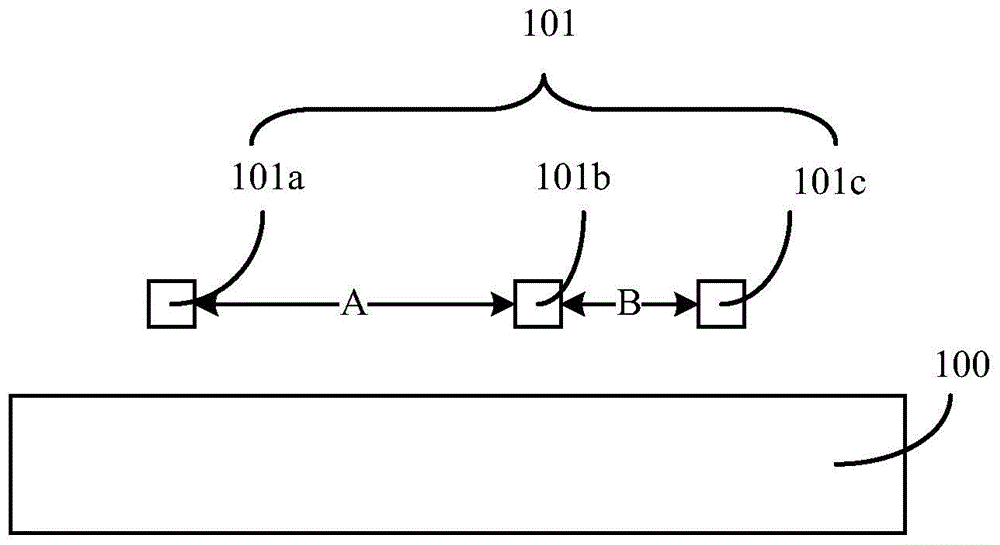
[0034] After research, please refer to figure 1 , figure 1 It is a schematic cross-sectional structure diagram of an embodiment of a nanowire structure, including: a substrate 100, a plurality of nanowires 101 suspended above the substrate 100 and arranged in parallel, the two ends of the nanowire 101 have supports on the surface of the substrate 100 Part, so that the nanowire 100 can be suspended on the substrate 100. Before forming the gate structure, the nanowire 101 needs to be annealed to make the cross section of the nanowire 101 circular.

[0035] However, according to the requirements of device design, the spatial distance between each nanowire 101 and the surrounding devices is different. For example, the distance A between the nanowire 101a and the nanowire 101b is larger, while the distance be...


PUM


Abstract

A formation method of a semiconductor device comprises the steps of providing a substrate, wherein the substrate possesses a first area, a sacrificial layer is arranged on the surface of the substrate, and a semiconductor layer is arranged on the surface of the sacrificial layer; forming at least three adjacent first grooves in the semiconductor layer and the sacrificial layer of the first area, wherein the first grooves expose out of the surface of the substrate, the semiconductor layer between the first grooves forms at least two parallelly arranged nano wires, the distances between the adjacent nano wires are same, and the nano wires comprise the device nano wires and the pseudo nano wires; removing the sacrificial layer at the bottoms of the nano wires to enable the nano wires to suspend above the substrate; after the sacrificial layer of the first area is removed, carrying out a first time annealing process to enable the cross-sections of the nano wires to be circular; after the first time annealing process, removing the pseudo nano wires. The morphology and performance of the formed semiconductor device are improved.

Description

technical field [0001] The invention relates to the technical field of semiconductor manufacturing, in particular to a method for forming a semiconductor device. Background technique [0002] With the rapid development of semiconductor manufacturing technology, semiconductor devices are developing towards higher element density and higher integration. Transistors, as the most basic semiconductor devices, are currently being widely used. Therefore, as the component density and integration of semiconductor devices increase, the gate size of transistors is also getting shorter and shorter. However, the shortening of the gate size of the transistor will cause the short-channel effect of the transistor, thereby generating leakage current, and ultimately affecting the electrical performance of the semiconductor device. [0003] In order to overcome the short channel effect of the transistor and suppress the leakage current, the prior art proposes a fully surrounded gate nanowire ...

Claims


Application Information

Patent Timeline
IPC IPC(8): H01L21/336B82Y10/00
Inventor 洪中山
Owner SEMICON MFG INT (SHANGHAI) CORP
Why Eureka
Try Eureka