Check patentability & draft patents in minutes with Patsnap Eureka AI!

Formation method of interconnection structure

A technology of interconnection structure and conductive structure, which is applied in the direction of electrical components, semiconductor/solid-state device manufacturing, circuits, etc., can solve problems affecting metal conductivity and small grain size, and achieve improved conductivity, high conductivity, and reduced The effect of electron scattering

Active Publication Date: 2015-11-25
SEMICON MFG INT (SHANGHAI) CORP
View PDF3 Cites 1 Cited by
  • Summary
  • Abstract
  • Description
  • Claims
  • Application Information

AI Technical Summary

Problems solved by technology

[0006] For the aforementioned copper damascene or double damascene process, since copper needs to be filled in smaller-sized holes or openings, the grain size inside the formed copper is generally relatively small, which will result in the above-mentioned grain size. The problem that the smaller particles affect the conductivity of the metal itself

Method used


Image

  • Formation method of interconnection structure
  • Formation method of interconnection structure
  • Formation method of interconnection structure

Examples


Embodiment Construction

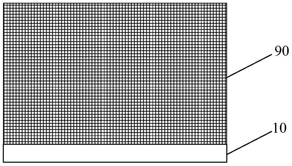
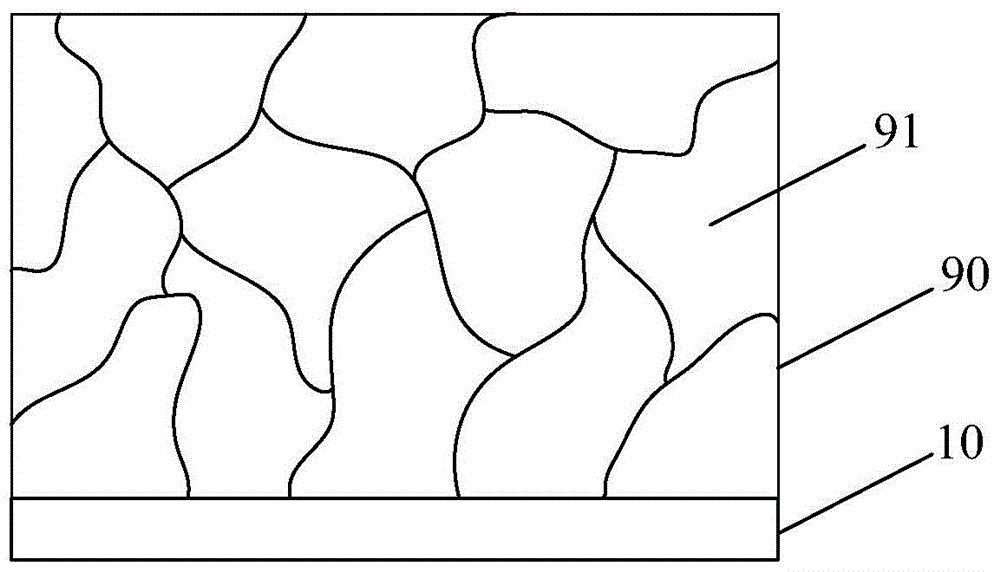
[0052] The metal grains formed by the method of forming the conductive structure in the interconnection structure in the prior art are all small, such as the conductive structure of the metal material formed by the Damascene or Dual Damascene process in the prior art (such as plugs or interconnection lines), the grain size inside the metal material is small, and the small grain size will reduce the conductivity of the copper material itself to a certain extent. The reason is that electrons are transported inside the metal When , the electrons will be scattered to varying degrees every time they encounter the grain boundary. For a fixed-size conductive structure, the smaller the grains, the more grains there are, and the more grain boundaries that electrons encounter during transport.

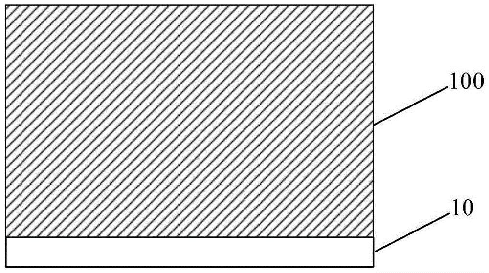
[0053] To this end, the present invention provides a method for forming an interconnection structure, including: providing a substrate; forming a first metal layer with grains of a first size on...


PUM


Abstract

The present invention provides a formation method of an interconnection structure. The formation method of the interconnection structure comprises the steps of providing a substrate; forming a first metal layer possessing the grains of a first size on the substrate, processing the first metal layer possessing the grains of the first size, and converting the grains of the first size into the grains of a second size, wherein the second size is greater than the first size; after the first metal layer possessing the grains of the first size is formed, adopting a plasma etching machine to etch the first metal layer, removing a part of the first metal layer to form a first conductive structure. The beneficial effects of the present invention are that: the grain size in the first metal layer is increased, so that when electrons are transmitted in the first metal layer, the probability that the electrons reach the boundaries of the grains is reduced, and accordingly, the phenomenon that the electrons generate the electron scattering at the boundaries of the grains is reduced to a certain extent; the conductivity of the first metal layer is improved, so that the interconnection structure having a higher conductivity is obtained.

Description

technical field [0001] The invention relates to the field of semiconductor manufacturing, in particular to a method for forming an interconnection structure. Background technique [0002] With the continuous development of integrated circuit manufacturing technology, people have higher and higher requirements on the integration and performance of integrated circuits. In order to meet these requirements as much as possible, new materials and manufacturing processes are used in the prior art to improve the performance of semiconductor devices in integrated circuits. [0003] For example, in the interconnection structure of semiconductor devices, copper gradually replaces traditional aluminum and becomes the main material of conductive structures such as conductive plugs or interconnection lines in the interconnection structure. The reason is that the resistivity of copper is lower than that of aluminum. The size is smaller, the melting point of copper is also higher, and the ...

Claims


Application Information

Patent Timeline
IPC IPC(8): H01L21/768
Inventor 张海洋任佳
Owner SEMICON MFG INT (SHANGHAI) CORP
Features
  • R&D
  • Intellectual Property
  • Life Sciences
  • Materials
  • Tech Scout
  • Unparalleled Data Quality
  • Higher Quality Content
  • 60% Fewer Hallucinations
Learn More