
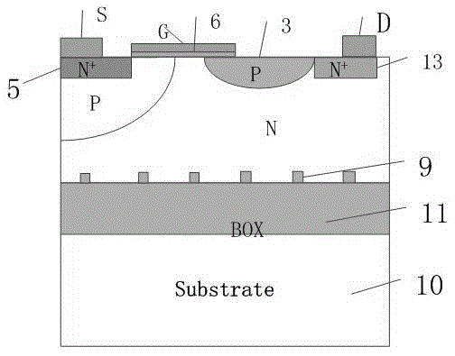
SOI high-voltage device provided with stepped shielding groove voltage-resisting structure and double-drain-electrode structure

A technology of withstand voltage structure and high-voltage devices, applied in semiconductor devices, electrical components, circuits, etc., can solve problems such as low breakdown voltage and self-heating effect

Inactive Publication Date: 2015-11-25
SHANGHAI RES INST OF MICROELECTRONICS SHRIME PEKING UNIV
View PDF2 Cites 0 Cited by
  • Summary
  • Abstract
  • Description
  • Claims
  • Application Information

AI Technical Summary

Problems solved by technology

But SOI high-voltage devices have two important disadvantages: lower breakdown voltage and self-heating effect
However, due to structural and process limitations, how to improve the vertical withstand voltage design has become a hot spot for SOI power devices.

Method used


Image

  • SOI high-voltage device provided with stepped shielding groove voltage-resisting structure and double-drain-electrode structure
  • SOI high-voltage device provided with stepped shielding groove voltage-resisting structure and double-drain-electrode structure
  • SOI high-voltage device provided with stepped shielding groove voltage-resisting structure and double-drain-electrode structure

Examples


Embodiment 1

[0017] Embodiment 1: an N-type LDMOS with a ladder-shaped shielding layer structure and a double-drain structure.

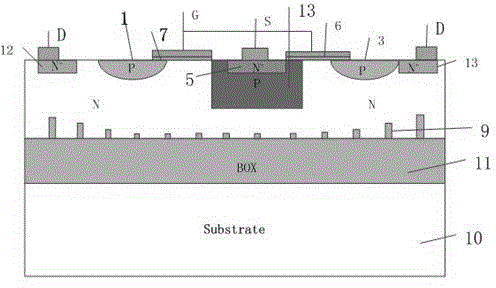
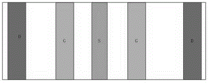
[0018] figure 2 It is a schematic structural diagram of an N-type LDMOS with a stepped shielding groove withstand voltage structure in the first embodiment of the present invention, Figure 4 It is a top view of the structure of an N-type LDMOS device with a stepped shielding groove withstand voltage structure in the first embodiment of the present invention.

Embodiment 2

[0019] Embodiment 2: an N-type LDMOS structure with a ladder-shaped shielding layer structure and ring drains and ring gates.

[0020] Figure 5 It is a top view of the structure of an N-type LDMOS device with a stepped shielding groove withstand voltage structure, a ring-shaped drain electrode, and a ring-shaped gate electrode structure in the second embodiment of the present invention. Compared with the double-drain structure, the annular drain and gate design further reduces the lateral electric field in the drift region, and the electric field distribution is more uniform, so the lateral breakdown voltage increases.


PUM


Abstract

The invention discloses a new SOI high-voltage metallic oxide semiconductor field effect transistor device which has a stepped shielding groove voltage-resisting structure and a double-drain-electrode structure and which can be used in an integrated circuit. The invention discloses a structure of a novel SOI high-voltage device, and the device improves a lateral breakdown voltage by utilizing a field plate technology and a double-RESURF technology of a surface P reduced-field layer. The device is characterized in that the device is provided with double drain electrodes, the area of a depletion region and the area of a drain region are increased, a transverse electric constant is reduced, and the lateral breakdown voltage is improved; and, for longitudinal voltage resistance of the device, the device solves the longitudinal voltage resistance through the structure of stepped shielding grooves formed on an interface of Si and buried layer SiO2.

Description

technical field [0001] The invention relates to the field of power devices, in particular to the SOI (Semiconductor On Insulator) high voltage device structure. Background technique [0002] SOI (Semiconductor On Insulator) high-voltage devices (referred to as SOI high-voltage devices) have higher operating speed and integration, better insulation performance, stronger radiation resistance and self-locking effect, so SOI high-voltage devices have been widely used in the field of ultra-large-scale integrated circuits. received widespread attention. But SOI high-voltage devices have two important disadvantages: lower breakdown voltage and self-heating effect. The lateral withstand voltage design of SOI high-voltage devices follows the mature Si-based device lateral withstand voltage design principles and technologies, such as the RESURF principle and junction termination technology. However, due to the limitations of structure and process, how to improve the vertical withsta...

Claims


Application Information

Patent Timeline
IPC IPC(8): H01L29/78H01L29/06H01L29/08
Inventor 张炯曲凯徐帆程玉华
Owner SHANGHAI RES INST OF MICROELECTRONICS SHRIME PEKING UNIV
Learn More