Method for preparing high-performance TFT

A high-performance, metal-layer technology, used in semiconductor/solid-state device manufacturing, electrical components, circuits, etc., can solve problems such as time-consuming and achieve low cost and improve efficiency.

Inactive Publication Date: 2015-12-02
FUDAN UNIV
View PDF5 Cites 0 Cited by
  • Summary
  • Abstract
  • Description
  • Claims
  • Application Information

AI Technical Summary

Problems solved by technology

Usually, the industry mainly uses rapid thermal annealing or furnace tube ann

Method used


Image

  • Method for preparing high-performance TFT
  • Method for preparing high-performance TFT
  • Method for preparing high-performance TFT

Examples


Embodiment Construction

[0038] In order to make the objectives, technical solutions, and advantages of the present invention clearer, the various embodiments of the present invention will be described in detail below with reference to the accompanying drawings. However, a person of ordinary skill in the art can understand that, in each embodiment of the present invention, many technical details are proposed for the reader to better understand the present application. However, even without these technical details and various changes and modifications based on the following embodiments, the technical solutions claimed by the claims of this application can be realized.

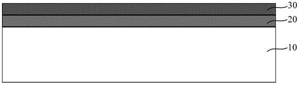
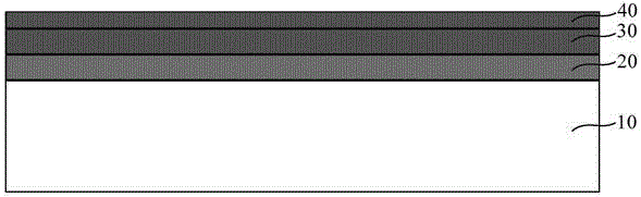
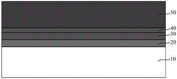
[0039] The first embodiment of the present invention relates to a method of manufacturing a high-performance TFT. The specific flowchart is as figure 1 As shown, in this embodiment, the method for preparing a high-performance TFT includes the steps:

[0040] S100: Provide a substrate, and sequentially form an active layer, a dielectric laye...


PUM


Abstract

The invention relates to the transistor manufacturing field, and discloses a method for preparing a high-performance TFT. In the method, a metal layer is formed on an activated layer, the activated layer is subjected to ion doping, and then a microwave annealing process is employed to activate doped ions. By utilization of high absorption effect of the metal layer to microwaves, the microwave annealing process efficiency is raised. The cost is low, and the method is helpful for batch production.

Description

Technical field [0001] The invention relates to the field of thin film transistor manufacturing, in particular to a method for preparing high-performance TFTs. Background technique [0002] Thin film transistors (TFTs) are widely used in display panels and other fields, and are named for transistors with electrical properties formed by depositing and patterning multilayer thin films on an insulating substrate. [0003] Early thin film transistors mainly used amorphous silicon as the activation layer. The rapid development of consumer electronics has higher requirements for TFT performance. In order to make the active layer have higher mobility, it is necessary to crystallize amorphous silicon. [0004] The crystallization of amorphous silicon is mainly achieved by heating up. Traditional thermal annealing (RTA) needs to be heated to 1000°C. Glass or organic substrates cannot withstand such high temperatures. Therefore, the main crystallization method used in the industry is laser ...

Claims


Application Information

Patent Timeline
IPC IPC(8): H01L21/336H01L21/3205H01L21/268
CPCH01L29/66757H01L21/268H01L21/32051
Inventor 付超超吴东平王言
Owner FUDAN UNIV
Why Eureka
Try Eureka