

Method for multi-board card to synchronically and sequentially read multi-path sensor data
A multi-channel sensor and sequential reading technology, which is applied in the direction of instruments, simulators, program control, etc., can solve the problem that the data of laser interferometer and grating sensor cannot be read at the same time
- Summary
- Abstract
- Description
- Claims
- Application Information
AI Technical Summary
Problems solved by technology
Method used
Image

Examples
specific Embodiment approach 1
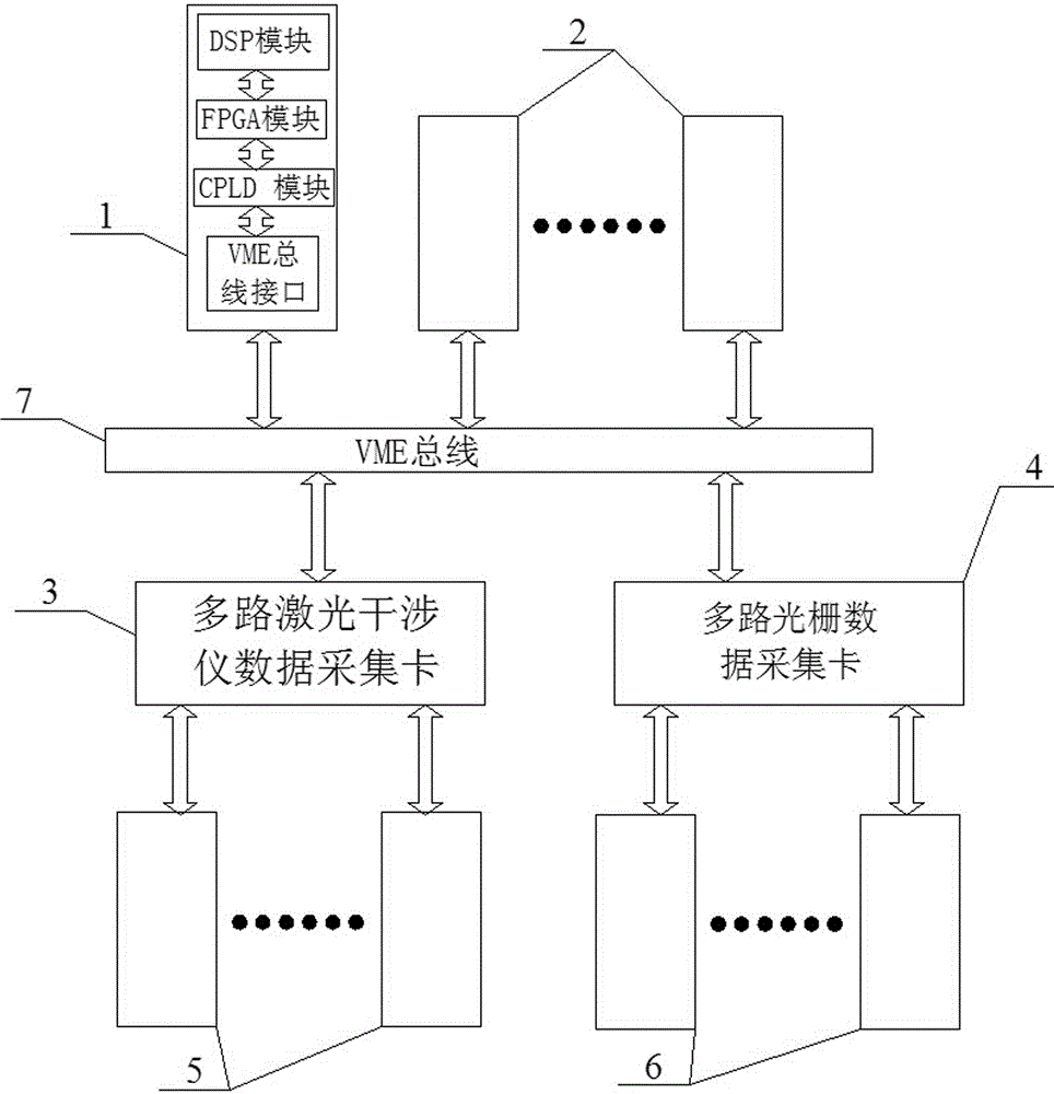
[0014] Specific implementation mode one: combine figure 1 Shown, illustrate the technical scheme of this embodiment, its method step is:
[0015] Step 1: The master card 1 of the motion control card, the slave card 2 of multiple motion control cards, the multi-channel laser interferometer data acquisition card 3 and the multi-channel grating data acquisition card 4 are all connected to the VME bus 7; The laser interferometer data acquisition card 3 updates the collected data from multiple laser interferometers 5 at a frequency of 10 MHz, and assigns these data to different address codes and stores them in the RAM of the multi-channel laser interferometer data acquisition card 3 The multi-channel grating data acquisition card 4 updates the data collected by a plurality of grating sensors 6 at a frequency of 10MHz, and stores these data in the RAM of the multi-channel grating data acquisition card 4 after giving different address codes;
[0016] Step 2: The DSP module in the ma...
PUM
 Abstract
Description
Claims
Application Information