Power diode and preparation method thereof

A technology of power diodes and anodes, applied in semiconductor/solid-state device manufacturing, electrical components, circuits, etc., can solve problems such as poor reverse recovery performance, achieve fast switching speed, shorten reverse recovery time, and reduce the effect of stored charge

Active Publication Date: 2015-12-09
西安国创电子股份有限公司
View PDF3 Cites 2 Cited by
  • Summary
  • Abstract
  • Description
  • Claims
  • Application Information

AI Technical Summary

Problems solved by technology

[0004] The purpose of the present invention is to provide a power diode, which solves the problem of poor reverse recovery performance existing in existing diodes

Method used


Image

  • Power diode and preparation method thereof
  • Power diode and preparation method thereof
  • Power diode and preparation method thereof

Examples


preparation example Construction

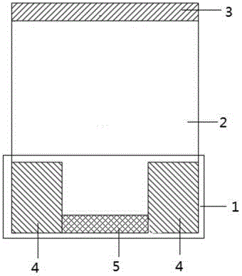
[0050] A method for preparing a power diode, including a cathode N arranged sequentially from bottom to top + Zone 1, voltage-resistant layer 2 and anode P + Zone 3, Cathode N + Zone 1 consists of two N + District 4, N + N zone 5 is set in the middle of zone 4, anode P + The dopants in region 3 are B ions and Ge ions, the content of Ge ions is 10% to 20%, and the N + The dopant of region 4 and N region 5 is P ion, the thickness of withstand voltage layer 2 is 10um-13um, the width is 6um-12um, N + The thickness of zone 4 is 3um~5um, the width is 2um~4um, the thickness of N zone 5 is 0.8um~1.2um, the width is 5um~7um, the cathode N + zone 1 and anode P + Area 3 uses ohmic contacts to form electrodes;

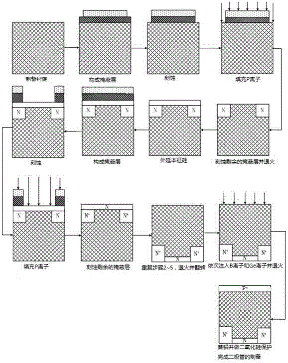
[0051] Specifically, follow the steps below to implement, such as figure 2 Shown:

[0052] Step 1: Prepare the substrate;

[0053] Preparing the substrate Use a silicon single crystal grown along the direction to make a substrate with a thickness of 13.0-13.1um;

[00...

Embodiment 1

[0071] A method for preparing a power diode, the power diode includes cathodes N arranged sequentially from bottom to top + Zone 1, voltage-resistant layer 2 and anode P + Zone 3, Cathode N + Zone 1 consists of two N + District 4, N + N zone 5 is set in the middle of zone 4, anode P + The dopants in region 3 are B ions and Ge ions, the content of Ge ions is 10% to 20%, and the N + The dopant of region 4 and N region 5 is P ion, the thickness of withstand voltage layer 2 is 10um, the width is 6um, N + Region 4 has a thickness of 3um and a width of 2um, N region 5 has a thickness of 0.8um and a width of 5um, and the cathode N + zone 1 and anode P + Area 3 uses ohmic contacts to form electrodes;

[0072] Specifically, follow the steps below to implement, such as figure 2 Shown:

[0073] Step 1: Prepare the substrate;

[0074] Preparation of the substrate Use a silicon single crystal grown along the direction to make a substrate with a thickness of 13.0um;

[0075] St...

Embodiment 2

[0092] A method for preparing a power diode, the power diode includes cathodes N arranged sequentially from bottom to top + Zone 1, voltage-resistant layer 2 and anode P + Zone 3, Cathode N + Zone 1 consists of two N + District 4, N + N zone 5 is set in the middle of zone 4, anode P + The dopants in region 3 are B ions and Ge ions, and the concentration of Ge ions is 0.5×10 22 cm -2 ~1×10 22 cm -2 , N + The dopant of region 4 and N region 5 is P ion, the thickness of withstand voltage layer 2 is 12um, the width is 9um, N + Region 4 has a thickness of 4um and a width of 3um, N region 5 has a thickness of 1um and a width of 6um, and the cathode N + zone 1 and anode P + Area 3 uses ohmic contacts to form electrodes;

[0093] Specifically, follow the steps below to implement, such as figure 2 Shown:

[0094] Step 1: Prepare the substrate;

[0095] Preparation of the substrate Use a silicon single crystal grown along the direction to prepare a substrate with a thick...


PUM


Abstract

The invention discloses a power diode which comprises a cathode N+ region, a voltage withstand layer and an anode P+ region successively from bottom to top, wherein the cathode N+ region comprises two N+ regions, arranged horizontally, and an N region therebetween. The invention also discloses a preparation method of the power diode, a Si material of the P+ region is replaced with a SiGe material, the cathode is arranged in the N+/N/N+ structure, the reverse recovery peak current is greatly reduced, the reverse recovery time of the diode is effectively shortened, and lower on-state voltage drop and higher switching speed can be obtained simultaneously. A break-through design can reduce the thickness of a drift region, the on-state voltage drop can be reduced, the storage charge is reduced, and power consumption of reverse recover is reduced; and according to the preparation method, expitaxy is combined with multi-time ion implantation to ensure that well N+ and N regions are formed, energy is greatly saved, and the utilization rate of electric energy is improved.

Description

technical field [0001] The invention belongs to the technical field of semiconductor devices, relates to a power diode, and also relates to a preparation method of the power diode. Background technique [0002] A power electronic device is a power semiconductor device that can realize high-efficiency application and precise control of electric energy, and is the basis of power electronic technology. The increasingly serious energy and environmental problems make people pay more and more attention to the conversion efficiency and quality of electric energy, and also guide the rapid development of power devices along the direction of high efficiency, high frequency, high withstand voltage, high power, integration, and intelligence. . Under many operating conditions, these devices require an anti-parallel diode to provide a freewheeling path, reduce the charging and discharging time of the capacitor, and suppress the high voltage induced by the instantaneous reversal of the lo...

Claims


Application Information

Patent Timeline
Patent Type & Authority Applications(China)
IPC IPC(8): H01L21/265H01L21/266H01L29/06H01L29/16H01L21/329H01L29/861
CPCH01L21/26506H01L21/266H01L29/0684H01L29/16H01L29/6609H01L29/8613
Inventor 马丽陈琳楠谢加强李伟
Owner 西安国创电子股份有限公司
Why Eureka
Try Eureka